Design of a microprocessor system. The main stages of design Programs for the design of microprocessor devices
The block diagram of the device is presented in Appendix A.
This microprocessor system consists of the following blocks: microprocessor, RAM, ROM, programmable parallel interface, analog-to-digital converter, timer, display.
The analog signals from the sensors are fed to the inputs of the analog multiplexer built into the ADC, which in each time interval switches one of the signals to the input of the analog-to-digital converter.
An analog-to-digital converter is used to convert an analog signal into a digital code that the microprocessor operates with.
The microprocessor accesses the ADC through a programmable parallel interface. Reads information from the outputs of the ADC, enters it into a RAM memory cell. In addition, based on the information received from the oil pressure sensor at the outlet of the station, the MP calculates the control action. This value is transmitted to the actuator in the form of a digital code.
RAM serves for temporary storage of information received from sensors and intermediate results of microprocessor calculations.
The system software is stored in ROM (Read Only Memory). The read operation is controlled by a microprocessor.
The program, which is stored in ROM, provides for the following system operations:
Sequential polling of sensors;
Control of analog-to-digital conversion of an analog signal;
Oil pressure regulation;
Indication and alarm;
Response to power loss.
System algorithm development
The block diagram of the algorithm is presented in Appendix B.
Initialization
At this stage, the control words are written to the RSS of the programmable parallel interface. PPI DD10 operates in zero mode. Ports work as follows: port A - input, port B - output, port C - output. PPI DD1 operates in zero mode. Ports work as follows: port A - output, port B - output, port C - output.
Polling sensors
The analog sensors are polled by the ADC. Discrete sensors through port A PPI 1 are interrogated by the microprocessor.
Save to RAM
The results obtained after polling the sensors are entered into a random access memory for temporary storage.
Control action
The microprocessor system analyzes the received data and generates a digital control action.
Concept development
Schematic diagram of the device is presented in Appendix D.
The address bus is formed using a buffer register and a bus driver. The register selection is made by the microprocessor's ALE signal. The bus driver is needed to increase the load capacity of the high byte of the address.
The data bus is formed using a bus driver, which is selected by applying the DT/R and OE signals.
The system bus is formed through the DD10 decoder by applying a combination of signals M / IO, WR, RD.
Table 1 - Control signals
The choice of ROM, RAM and other devices occurs using the lines A13-A15 of the address bus through the decoder. ROM cells are located from address 0000h.
Table 2 - Device selection
|
Device |
|||
The selection of the port or register of the PPI control word is carried out through the lines A0, A1 of the address bus. Discrete sensors are supplied to the inputs of port A PA0-PA7 PPI DD12; to the inputs of port B - with ADC; LEDs are connected to the inputs of port C.
The analog multiplexer is used to select the device from which information is read. The analog multiplexer is built into the ADC. The bit width of the ADC coincides with the bit width of the data bus and is 8 bits.
Resistors R2-R4 are used to convert a unified current signal of 4 ... 20 mA into a voltage of 1 ... 5V.
The processes of automation of technical equipment have captured a large part of the entire organization of production. They are used everywhere in machine tools, machines and mechanisms, robotic complexes. New technologies significantly increase labor productivity, reducing the impact of the human factor on risks in production. The technical level and quality of products are also improved. Microprocessor systems - at one time was an innovative technology. But now this is already commonplace, because devices that are made using microprocessors have higher performance compared to devices made on separate logic circuits, with the economic benefit of the former.
Standardization of the development process simplifies analysis and research in this area. It also makes the current state and the possible result clear. Today's embedded microprocessor companies use field-programmable logic integrated circuits (FPGAs) and computer-aided manufacturing systems for fast and organized design. With the help of FPGAs, real-time debugging and testing is also possible. The annual CAD update allows you to spend less and less time on monotonous and monosyllabic work, while avoiding obvious mistakes. This allows you to abstract to higher levels of the system and solve difficult problems.
The process of developing embedded microprocessor systems can be represented as two routes of successive design stages. The first route is the development of the hardware of an embedded microprocessor system. The second route is software design (Fig. 1).
Figure 1. Design stages
But not all stages of the route are required. Modeling of the hardware of the system during development may not be carried out. Therefore, some steps can be excluded: preparation of the modeling specification, generation of models, functional and temporal modeling. At the same time, it should be taken into account that modeling the hardware of the system increases the efficiency of the design process as a whole due to earlier detection of possible errors and their elimination.
Typical design steps for microprocessor systems include:
- Formalization of various system requirements. It is necessary to draw up external specifications, terms of reference (TOR) for the system, notes of the system image by the developer in the documentation, lists the functions of the system.
- Development of the structure and architecture of the system elements. It is necessary to determine the interaction between hardware and software, the functions of peripherals and software shells, to choose microprocessor solutions on the basis of which the system will be implemented, to determine the time characteristics.
- Development and production of hardware and software of the system. It is necessary to develop the structure and circuit diagrams, make a prototype, and debug it in the conditions of basic operating modes. Software development should consist of algorithms, writing source code, translating source programs into object programs, software debugging, and simulation.
- General debugging and acceptance tests in working conditions.
The human factor allows for malfunctions and poor design decisions. There are also hardware defects in the devices. For example, the following sources of errors in stages are possible:
Stage 1. Logical inconsistency of requirements, omissions, inaccuracies of the algorithm.
Stage 2. Omissions of functions, omission of some information flows, inconsistency of the protocol for the interaction of hardware and software, incorrect definition of technical requirements, incorrect choice of microprocessor solutions, inaccuracies of algorithms.
Stage 3. When developing equipment - omission of some functions, incorrect interpretation of the terms of reference, flaws in synchronization schemes, violation of design rules; when developing software - omissions of some functions of the terms of reference, inaccuracies in algorithms, inaccuracies in coding; in the manufacture of a prototype - malfunctions of components and peripherals, malfunctions of installation and assembly.
Each of the listed sources of error can lead to a large number of physical or subjective faults that need to be further identified and eliminated. Detection and localization of a malfunction is complicated for several reasons: firstly, due to malfunctions, there may be several; secondly, the uniformity of symptoms of various problems. Since there are no models of subjective faults, this task is not formalized. It is possible to solve with the help of expert systems - a database with existing problems and their solution based on practical experience.
Subjective faults differ from physical faults in that they no longer occur after detection, localization and correction. But subjective faults can be introduced during the system specification development phase, which means that even after the system has been thoroughly tested against its specifications, there may be subjective faults in the system.
The design process is an iterative process, which means that if errors are not completely eliminated at one stage, they may appear at the next. It is necessary to detect malfunctions as early as possible, for this it is necessary to control the correctness of the project at each stage of development. For example, faults discovered at the final stage of acceptance and delivery of the project can lead to correction of specifications, and, consequently, to the beginning of the design of the entire system. Changes in the terms of reference (due to understatement and lack of information about the system) lead to the same consequences.
The main methods for controlling the design correctness are: verification, modeling and testing.
Verification allows you to detect not only current errors, but also potential errors that may appear in future projects using blocks. But it requires a separate technical task and relevant skills and is suitable for large projects. On small projects, object behavior modeling and testing are more often used. this option is cost-effective and does not require a lot of resources.
Correctness control is achieved at each design stage by the need to conduct simulations at various levels of system abstraction and verify the correctness of the implemented part of the model through testing. The functional specification can be modeled and tested experimentally to determine the expected result. It can also be analyzed by a team of experts. After the approval of the functional specification, the development of functional tests of the system begins, designed to establish the correct functioning of the system in accordance with its functional specification. It is most efficient to develop tests based entirely on this specification, as this makes it possible to test any system implementation capable of performing the functions specified in the specification. This method is similar to others, where tests are built in relation to specific implementations, but more accurately compares the expectation and development result.
Once an error has been detected, its source must be localized in order to be corrected at the appropriate level of the abstract representation of the system and in the appropriate place. Incorrect determination of the source of the error or making adjustments at another level of the abstract representation of the system leads to the fact that information about the system at the top level becomes erroneous and cannot be used for further debugging during the production and operation of the system.
Automating the monotonous work of developing test programs shortens the build and debug period by getting tests earlier (because they can be generated as soon as the system requirements are formed) and allows the designer to change specifications without rewriting all the test programs. In practice, the development of tests is of lesser priority than the project, so test programs appear much later than its completion.
Thus, taking into account the nuances of microprocessor design, one can easily bypass the "pitfalls" during development. The use of programmable logic integrated circuits (FPGAs) makes it easier to debug a batch that has not yet been released and allows you to test the design and fix bugs. And computer-aided manufacturing (CAD) systems simplify development, allowing you to reallocate resources more rationally.
Bibliography:
- SibGUTI [Electronic resource] / Designing a microprocessor on an FPGA - Access mode: http://ict.sibsutis.ru/sites/csc.sibsutis.ru/files/courses/mps/mp.pdf-free. - head. from the screen. - language Russian (accessed 22.12.2017).
- Zotov V. Embedded Development Kit is a system for designing embedded microprocessor systems based on FPGA series FPGAs from Xilinx. 2004. No. 3.
1. functioning,design and architecturemicroprocessor devicesand systems
1.1. Are commoninformation about microprocessor technology
Basic concepts anddefinitionsmicroprocessor technology
Microprocessors and microcomputers are mass products of the electronics industry. Knowledge of the basics of microprocessor technology is necessary for engineers of any profile, especially system engineers, design engineers, process engineers of computer systems (CS).
Microprocessors (MP) are widely used in modern aircraft and radio electronic devices (REU), technological control systems, flexible automated and other industries. The use of MP has a positive effect on increasing labor productivity, improves the quality of equipment for various purposes. Thanks to the use of MP and microcomputers in technical systems, the functionality of the equipment has expanded, its reliability and stability of operation have increased, and the quality of information processing has improved.
The prospects and possibilities of using MPs and microcomputers in computing systems have not yet been fully disclosed. The production technologies and architecture of the MP are constantly being improved. So, the bit depth of modern single-chip MP reaches 64 bits. When using MPs and microcomputers, developers must be able to evaluate the capabilities of their architecture and technical characteristics, as well as to be proficient in programming languages of different levels. Assembly language is widely used to create system software. In order to ensure high productivity of programmers, data processing tasks are solved using high-level languages (for example, C). Modern engineers - specialists in computer technology need knowledge in the field of both MP architecture and programming of electronic devices in languages of different levels.
The basic concepts in microprocessor technology are such concepts as: "microprocessor", "IC", "IC", "LSI", "VLSI", "microprocessor set of LIS", "microprocessor device", "microprocessor system", "microprocessor equipment”, “microcomputer” (general purpose and specialized), “embedded microcomputer”, “personal computer”, “household personal computer”, “professional personal computer”, “microcontroller”, etc.
In addition, in microprocessor technology, concepts related to computer technology are used, and in particular "backbone", "bus", "interface", "system interface", "peripheral interface", "adapter", "protocols", "interface line " and etc.
When studying software in microprocessor technology, general concepts are used that coincide in name with the concepts of describing software in computer technology, in particular, “algorithm”, “program”, “software”, etc.
One of the main, basic concepts of microprocessor technology is "microprocessor".
Microprocessor- it complexsoftware controlled device,designed to process digital information andprocess control of this processing, made in the form of one or more integratedmicrocircuits of the increased degree of integration (BIC or SBIWITH).
Integrated circuit (IMS) is a microelectronic device that performs a certain function of converting, processing signals and (or) accumulating information, which has a high internal packing density of electrically connected elements (or elements and components) and (or) crystals and is considered in the aspect of testing, delivery and operation requirements electronics products as a whole.
Semiconductor IC- an integrated microcircuit, all elements and interelement connections of which are made inside and on the surface of the semiconductor.
Digital IC- an integrated circuit designed to convert and process signals that change according to the law of a discrete function.
Degree of integration- an indicator of the degree of complexity of the IC, which is characterized by the number of elements and components that are contained in it. The degree of integration is determined by the formula k= log N, where k- coefficient that determines the degree of integration, the values of which are rounded to the largest integer; N- the number of elements and components of the IC.
Large integrated circuit (BIWITH)- an integrated circuit that contains 500 or more elements manufactured using bipolar technology, or 1000 or more elements manufactured using MOS technology, extra large integralscheme (SBIWITH)contains over the elements.
SetBIS- a set of LSI types that perform various functions that are compatible in architecture, design, electrical parameters and provide the possibility of their joint use in the manufacture of microprocessor technology.
microprocessor kit (IPC)- a set of microprocessor and other ICs that are compatible in architecture, design and electrical parameters and provide the possibility of their joint use.
The microprocessor is described by numerous parameters inherent in both electronic devices (speed, power consumption, dimensions, weight, number of power levels, reliability, cost, package type, temperature range, etc.) the number of internal registers, the presence of a microprogram level, the type of stack memory, the composition of the software, etc.).
microprocessor device ( MPU) - functional and constructivea finished product, which is a schematic and constructiveconnection of several microcircuits, including one or more microprocessorsdesigned to perform one ormultiple functions: receiving, treatment,transfer, transformation of information and management.
MPU has unified connecting characteristics (interface, design, etc.) and functions as part of a specific technical system.
Microprocessor system ( MPS) - it a large number offunctional devices, one ofwhich have a microprocessor.
The microprocessor is the core of this system and performs the functions of a central control device and an arithmetic-logical data conversion device. All MPS devices have a standard interface and are connected to a single information highway.
Microprocessor technology - microprocessors and computing devicestechnology (VT) and automation, made on their basis.
These are the most generalized concepts of computer technology. Today, almost all VT is built on the basis of microprocessor devices.
General purpose microcomputer - it microcomputers that have largeoperational resources adapted to handle a variety ofnumerical and textual data and intended for use in computingcenters.
This is the most common class of microcomputers, which is the base for personal computers.
Specialized computers - it computers designed to implement a specificspecific algorithm:Fourier transforms, correlation calculationsfunctions andothers
They are narrow-profile computers with a limited number of system commands.
built-in microcomputer (microprocessor device) - processing unitdata andcontrols intended for use in domesticinstruments, process control systems orcontrol, computer peripherals, office equipment, etc.
Most of these computers are used in household appliances (TVs, radios, washing machines, etc.)
Personal computer (personal computer) - dialogue systemfor personal use, implemented onbased on microprocessormeans, small-sized external storagedevices and data recording devices,which provide access to all computer resources using a developed programming system in high-level languages.
This is a small in size and cost universal microcomputer designed for individual use. Household personal computers act as a home information center. Professional personalcomputers designed to automate various operations of processing large amounts of information at the workplace of a specialist.
microcontroller- controlled device, made on one or more chips, the functions of which are logical analysis and control.
Classification of microprocessors and their main parameters
By the number of LSIs, single-chip, multi-chip and multi-chip sectioned MPs are distinguished.
Single-chip MP implement all the hardware of the processor in the form of a single LSI or VLSI. A single-chip MP has a fixed bit depth, a set of commands, and is structurally made in the form of a single integrated circuit (IC). All operations carried out by it are determined by a set of MP commands. A feature of a single-chip MP is the presence of an internal highway for transmitting internal information data and control signals. The capabilities of these MPs are limited by the hardware resources of the crystal and package, but with an increase in the degree of crystal integration and the number of package pins, the parameters of the MP are continuously improved.
V lotcrystal MP the logical structure is divided into functionally complete parts, which are implemented as separate LSI and VLSI or separate crystals in one VLSI.
Multichip partitioned MP consist of a set of microprocessor sections.
microprocessor section- it microprocessor integrateda circuit that implements a part of the MP and has the means of a simple functionalassociationswith the same type or other microprocessor sections for building complete MP, MPU or microcomputers.
Sectioned MPs are controlled by firmware. Sectioned MPCs include LSI series: K1800, KR1802, KM1804, etc. Their main purpose is to create high-performance multi-bit MPs and MPCs, on the basis of which various control computer systems are implemented.
The basis of the IPC BIS is the basic set of ICs of one series. It can consist of a single-chip MP IC with a fixed bit depth and a set of commands or a set of single-chip MP LSI. To expand the functionality of the MP, the basic MPC LSI is supplemented with other types of LSI: RAM, ROM, PROM, interface integrated circuits, external device controllers, etc.
According to the type of processed signals are distinguished digital and analog MP. In both types of MT, information processing is digital. In digital MPs, purely digital signals are processed, while in analog MPs, an analog-to-digital device (ADC) and a digital-to-analog converter (DAC) are built-in for processing analog signals. In them, the input analog signals are transmitted to the MP through the ADC, processed in digital form, converted to analog form in the DAC and output.
Choice of microprocessor kit
for the design of computing devicesand systems
Choosing an IPC for a specific computing device or system is the most difficult task. This is due to the constant increase in the number of IPCs and LSIs in them.
When choosing an MPC, the equipment must meet certain requirements: work in real time; increased reliability; noise immunity; ease of maintenance; the presence of a fixed set of tasks that are solved repeatedly throughout the life of the equipment.
The choice of the IPC is carried out according to three main criteria:
1) in the aspect of software development, it is necessary to analyze the bit depth, the number of general-purpose registers available for use, the set of commands and addressing methods, the presence and organization of the stack;
2) regarding system design, it is necessary to determine: the type of MP architecture (sectioned or single-chip), the type of control organization (microprogram or with hard logic), the presence of logically joint LSI from other sets, the speed of the MP, the possibility of interruption and direct access to memory, the availability of an automated design;
3) from the point of view of the development of MPS hardware, it is necessary to take into account: the electrical compatibility of the LSI, the number of power sources and power dissipation, the size and type of package, the number of pins, the operating temperature range, etc.
The choice of an RPC for a particular application is often made on the basis of the technology by which it is manufactured.
Questions and tasks
1. What factors determine the use of MP and microcomputers in production systems?
2. How do single-chip MPs differ from multi-chip ones (non-sectioned and sectioned)?
3. What are the general parameters characterize MP, MPU and MPS?
4. On what grounds are MPs characterized?
5. Name the main parameters of modern MT.
6. What are the criteria for choosing microprocessor sets when designing computing devices and systems?
1.2. General issuesorganizations andfunctioningmicroprocessor devicesand systems
Structure of microprocessor devicesand systems
Any MPS consists of an MP, a memory system, an information input-output system, and a system for interfacing with an object of control or control.
microprocessor and plays the role of a central control device and a device for arithmetic-logical data transformations.
Memory is physically implemented as a system that consists of several levels.
Persistent storage devices (ROM) are intended for long-term storage of pre-recorded data and are used only in read-out mode. They are energy independent.
Random Access Memory (OZP) work in the modes of online writing and reading data with a speed that approaches the speed of the processor. They are energy dependent.
External storage devices (Inmemory) perform the functions of storing large amounts of information, contain drives on floppy and hard magnetic disks, compact disks (laser), etc.
Devicesdata entry (ID) designed to transfer data from the outside to MP registers or memory. Among them are a keyboard, various control panels, magnetic and laser disks, etc.
Data output devices (UVv) designed to accept data transmitted from MP registers or memory cells. These are displays, printing devices, VZU, control panels, plotters (plotters), etc.
To interface the object of control or control with the MPU or MPS, the equipment must include sensors and actuators. To connect them to the MPU, whether the MPS use blocksconjugation, that perform interface matching functions. Sometimes these blocks are called communication devices with the object (USO).
Interfaces of microprocessor devicesand systems
The architectural capabilities of the MPS largely depend on the type of interface.
Unified interface is a set of rules thatunified principles of interaction between MPS devices.
The interface includes hardware for connecting devices (connectors, connections), specification of the nomenclature and characteristics of connections, software, descriptions of the nature of the interface signals and their timing diagrams, as well as a description of the electrophysical parameters of the signals.
The main task of the interface is, on the basis of unification, to ensure the compatibility of hardware, software and constructive means that predetermine the specified quality of automatic interaction of different functional elements in a single information processing process in the MPS at the stages of collecting, converting, saving and issuing results and control actions.
The MPS architecture is mainly defined by three interface layers: system, machine-to-machine, and small interface (peripheral device interface).
System interface ensures the integration of the main modules (blocks) of the MPS into a single system for equal exchange of information with the processor and OZP.
System interfaces are divided into concentrated (PC interfaces), locally concentrated (Q-bus) and local (Unibus).
Machine to machine interface provides the construction of multiprocessor systems and local and distributed systems and networks.
Small interfaces take into account the difference in the physical principles of operation of groups of peripheral devices and ROM. Small interface controllers provide access to the system interface. In this case, the controllers of peripheral devices and ROM go to the corresponding small interface.
Management of microprocessordevices (systems)
Temporal coordination of information signals in the MPU is carried out using special signals coming from the MP control device. MPU or MPS operates synchronously with the advent of clock signals. The simplest action that is performed in the MPU (MPS) is called state. It covers one period of the clock signal - clockedinterval or beat.
A certain number of clock intervals is machinecycle. A single memory or I/O device access requires one machine cycle. In one cycle, the instruction or data is fetched, as well as the address code (possibly the instruction or data byte and the address code byte).
Machine cycle- part of the team (sometimes the whole team). With the beginning of each machine cycle, a synchronization signal appears on the synchronization pin of the MP. It is transferred to the storage device (memory) and (or) to the input / output device (I/O) and “notifies” about the beginning of a new machine cycle, as a result of which the timing of the operation of these devices with the operation of the MP is achieved.
Scheme 1. Team structure
Team Cycle- the time interval required to fetch the command from memory and execute it. It consists of one or more machine cycles. their number, as a rule, is equal to the number of MT accesses to the memory or to one of the ICUs. The command structure is shown in Diagram 1.
control device performs the functions of control and synchronization, that is, it controls the change in the states of the MP in the required sequence, coordinating them with the signals of the clock generator. It consists of a control finite automaton designed to control processes inside the MP, and a circuit that, receiving signals from outside, generates signals that control the system.
The command code is decrypted, turning into binary signals that act on the MP modules and blocks involved in the execution of this command.
The command cycle is divided into two phases: the fetch phase and the execute phase.
Sampling phase- the automaton sets the beginning of the next cycle, according to which the number in the program counter is transferred to the address buffer register. From there, via the address bus, the instruction's address code is sent to memory, where it is decrypted. After the “read” signal from the memory cell, the command word is read and transmitted over the data bus to the buffer data register, from which it is transferred to the command register, and then decrypted.
Execution phase- the control device generates a sequence of signals necessary to execute the command. During this time, the counter data is incremented by one. This forms the address of the next instruction to be executed.
Reading or writing a word occurs over a certain time interval, which is called the access time. The time interval that is spent accessing the memory and receiving a ready signal from it is called the ready waiting cycle. It forms part of the machine cycle.
The exchange of information between the MP, the memory and the IUV is implemented mainly in three modes: program-controlled exchange, exchange in the interrupt mode, exchange in the direct access mode.
Software-controlled exchange. In this mode, the MP determines whether the memory or peripheral device (PU) is ready to perform an I / O operation, to start software data transfer. Air-blasters must have hardware for generating signals about the internal state. The MP reads this information and, based on the analysis of the result, concludes that the device is ready to exchange information. In the future, in accordance with the interface protocol, data is exchanged.
interrupt mode. It is used when it is necessary to immediately transfer data between air-blast and MP (reaction to unexpected occurrence of external conditions). In this case, the MP must interrupt the operation of the main program and start executing the program for servicing the external device. This mode is called interrupt. MP interrupts are only possible when the MP is allowed to respond to interrupt requests.
After receiving the interrupt signal, the MP completes the current operation, transfers all the information of the internal data and control registers to memory, and proceeds to the interrupt service routine. After the end of the exchange of information on the interrupt, the state of the MP is restored, which existed at the beginning of the interrupt.
There are three types of interrupts: simple, vector and priority.
Simple interrupt notifies that some input/output device requires MP service.
Vector interrupt makes it possible to recognize the type (level) of the interrupt required by the peripheral. The vector specifies the specific address of the device.
Priority interrupt consists in the fact that, in addition to interrupt recognition, the priority in servicing interrupting devices is determined.
Direct modememory access. Sometimes there is a need to exchange information outside the MP. This is due to a decrease in the time spent on exchanging data arrays. In this case, the hardware of the MPP or MMS includes a direct memory access controller that manages data transfer, freeing the MPU from these functions.
DMAs are connected in parallel to the processor. The separation of these channels is carried out using the tri-state logic of controlling the state of the MPS buses. The MP during direct memory access transfers its original circuits to a high-impedance state and is isolated from the system, which is similar to breaking the information channel. The state of the internal registers is preserved as it was at the time of the direct access channel request.
There are several ways to implement direct memory access. All of them provide the highest data exchange rate in comparison with the program-controlled exchange mode. Most often, the direct memory access mode is implemented with the stop of the MP and the increase (lengthening in time) of the MP cycle.
Stop method is based on the fact that in this state the MP is disconnected from the system buses for the duration of the data transfer. Before switching to the stop state, the MP completes the execution of the current command and lingers in this state for several cycles, until the tires are free. According to this scheme of direct memory access, the MP, being disconnected from the buses, does not respond to interrupts, which in some cases may be unacceptable for the MPS.
Capture method consists in serial data exchange. High-speed air-blasters exchange only one word; their service request is satisfied by delaying the execution of the current instruction by one machine cycle while the MP is in a state of transition from one machine cycle to another. In this DMA mode, the MP pauses for only one machine cycle to transfer each data word, after which control returns to the MP.
address space. Mechanism and methods of addressing
Address space MPU (MPS) - set of operational addressesmemory andROM that is available to programs executed by the MP.
The size of the address space of the MP RAM is one of the quantities that significantly affect the performance of the MPS as a whole.
Address space size - value,which is determined by the maximumaddress size and is expressed in units of the minimumthe number of memory elements that are addressed - in bytes, or in largeunits (KB, MB, GB).
If the address in the MPU is formed in the form of a 16-bit word, then the address space is 64 KB, a 20-bit word is 1 MB, etc. Sometimes, to simplify information links between the components of the MPU and facilitate programming of I / O procedures, register addresses are placed in the address space MP and UVV. There are no input/output commands as such. Addresses to the MP and UVV registers are identical to access to memory cells.
When a word, a 2-byte address, is formed, the byte with an even (lower) address is called the lower one, and the byte with the odd address is called the higher one.
Often, the LPA address space is represented as a diagram, which indicates the general range of addresses. This range can be divided into subranges that correspond to the standard sizes of structural modules, chips, different types of memory (RAM, ROM, etc.) or their specific purpose.
In the MP command system, address commands occupy a significant place.
Address command - the team in whichone or both of its operands arein working memory.
One of the reasons for such an organization of the instruction is that it is impossible to write the full physical address directly in one operand of the instruction due to restrictions on the length of the instruction. Therefore, only a certain value is placed in the operand, with the help of which the actual address of the instruction is calculated.
In general, the addressing mechanism is largely determined by the capabilities of the MPU (MPS) to efficiently process information with a minimum number of accesses to the RAM. In MPU (MPS), commands of two or more words are often used.
To limit the length of the address word, various addressing methods are used, which make it possible to:
1) determine the full address of the memory cell with fewer bits than the length of the command is reduced;
2) access memory cells whose addresses are calculated during processing, which provides access to memory expansion devices;
3) calculate data addresses relative to the position (current address) of the instruction so that the program can be loaded into any memory location without changing the address in the program.
All addressing modes can be divided into two groups:
1) modes in which the execution address is determined by one code value in the command;
2) commands that use the contents of the address part of the command and one or more registers to form the execution address.
The first group includes direct, direct register, indirect, indirect register, direct, auto-increment and auto-decrement addressing, and the second group includes basic, relative, stack, virtual addressing.
direct addressing. Operands are fetched from memory (registers) at the address written in the instruction. However, specifying a direct address requires many bits to describe in a large address instruction. To reduce it, some microcomputers use short direct addressing, providing access to a limited part of the address space. If the addresses in the command are not symbolic (specified by links), but absolute, then such direct addressing is called absolute.
Direct register addressing. V The instruction code stores the name of the register in which the operand is located. Direct addressing is not flexible enough, because it does not allow you to perform the address modification procedure necessary to ensure the movement of programs in memory and the convenience of working with arrays.
indirect addressing. The operand from memory is selected indirectly - through a memory cell. The instruction code contains a memory address pointer. When executing instructions with such addressing, memory is accessed twice: first, the address is selected, and then the operand. Thus, without changing the command code, it is possible to change the address stored in the memory area pointed to by the command code field.
Indirect register addressing. In terms of speed, it approaches direct addressing, since the indirect address is selected from the processor's internal register and does not require an additional memory cycle. In this addressing scheme, a register or register pair contains the address of the operand. The registers are loaded using commands with direct addressing. The use of the indirect register addressing mode makes it possible to calculate the memory address during program execution, which is necessary in data transfer procedures, when viewing array elements, etc.
direct addressing. The operand is in the instruction code. Commands in this case can consist of two or three words.
Autoincrement and autodecrement addressing. The executable address is calculated in the same way as with indirect register addressing, and then the contents of the register are incremented. In a byte-addressed microcomputer, the contents of the register must be increased by 1 to indicate the next byte, and by 2 to indicate the address of the next word, with the size of the operand determined by the opcode. In auto-decrement mode, the operand address is formed by subtracting 1 or 2 from the address register. The difference from auto-increment addressing is that the subtraction occurs before the contents of the register are used as the execution address. The combination of auto-increment and auto-decrement modes makes it possible to effectively use any register as a stack pointer. This addressing is also used when organizing loops and in operations with string variables.
base address. Programs that contain instructions with absolute addresses cannot be moved in memory without modifying the addresses. You can ensure the movement of programs in memory using basic addressing, with the help of which the address of the operand is calculated by adding the contents of the base register - a positive or negative offset and the address located in the instruction code.
Relative addressing. The executable address is formed by adding the base address to the instruction's address field. As the base address, the content of the program counter is used. Using relative addressing makes it possible to build programs that move independently in memory due to the fact that they always specify an offset relative to the contents of the program counter. The offset is interpreted as a two's complement signed integer that provides a jump in either direction.
stack addressing. Indirect register addressing with auto-increment or auto-decrement (auto-increment or auto-decrement), in which the register with the operand address pointer is specified implicitly (there are such instructions where the location of the operands and the result is fixed - implicit addressing). The memory location pointed to by the contents of an implicitly defined register (stack pointer) is called summit stack. Stack addressing provides special access to a piece of memory called stack, which is based on the principle of “last in, first out”. To access the stack, instructions are used that write information to and from the stack. If the instructions that write information to the stack decrement the contents of the stack pointer, and the instructions that remove information from the stack increment, then we say that the stack works to decrease, otherwise - to increase.
virtual addressing. Each user of memory (operating system or person) while solving an applied problem manipulates virtual addresses, which creates the illusion of memory of unlimited capacity, although the real RAM of the system has a limited capacity. The illusion is created due to the virtual addressing mechanism, which is based on the dynamic redistribution of memory pages between the system's main memory (OZP) and external memory.
For each user, the operating system creates a table of correspondence between virtual and physical pages. If a physical page is accessed that is not in the main memory, then it is removed from the external memory and loaded into the main one, and the unnecessary page is “hidden” in the external memory. Virtual memory, or simply system memory, can be divided into segments in which information is stored according to functional features. For example, in one segment - commands, in the second - data, in the third - a section of the stack. Or, in one segment, in which writing is prohibited, - the operating system kernel, and in the second, in which writing and reading are allowed, - user programs. Thus, with the help of the segmentation mechanism, the problems of memory protection are solved.
Segmentation was implemented in the K1810VM86 MP, and virtual addressing was implemented in the IAPX286 MP (Intel) and 68010 (Motorola).
command system. In general, a command is understood as a single step in the operation of an executive device in the form of an instruction in machine language. The command defines the operation to be performed and its attributes: the type of operation to be performed in the given work cycle; address of one or two operands involved in the operation; location of the result of the operation; the location of the next command. Due to the small capacity of the MP, such information is difficult, and sometimes impossible, to indicate in one machine word. Therefore, a command can consist of several machine words.
In general, the following types of commands are distinguished:
1) transfer - unidirectional (register-register, memory-register, register-memory, memory-memory), exchange (register-register, memory-register, memory-memory), input / output commands;
2) arithmetic;
3) logical;
4) processing bits;
5) those that change the sequence of calculations - jumps (unconditional, conditional), calls to subroutines, returns from subroutines, software interrupts.
Questions for self-examination
1. Describe the generalized structure of MP and MPS.
2. On what grounds are the MPU and MPS interfaces classified?
3. What functions does the MP perform when processing a command (instruction) during the sampling phase, the execution phase?
4. Under what circumstances is the exchange of information between the MP and storage devices carried out in the mode of interruption or direct access to memory?
5. On what parameters of the MP does the size of the address space depend?
6. Using appendix 1, give examples of address commands with direct, indirect, immediate, base, relative, auto-increment, stack, and virtual addressing.
7. What information does the command code carry in the MP command system?
1.3. Process Formalizationdesignmicroprocessor devicesand systems
Aspects and levels of design
When designing MPU and MPS, in many cases they use block-hierarchical approach, in which The system being designed is divided into hierarchical levels. At the highest level, the most undetailed view is used, where only the general features and features of the system being designed are displayed. At the next levels, the level of detail increases. In this case, the MPS is considered as a set of individual blocks. At each level, tasks of a certain complexity are formulated and solved, which are implemented using the design tools available at this level. The block assignment should be such that the documentation for each individual block is understandable to one designer.
So, the block-hierarchical approach makes it possible to distribute the complex tasks of designing a large-scale MPS into groups of small-scale tasks, and within the group, different tasks can be solved in parallel.
In accordance with ESKD, when designing devices and systems, structural, functional and schematic diagrams are used.
It is conditionally possible to distinguish horizontal and vertical levels in the simulated design scheme (Table 1). The vertical levels are called aspects. There are such aspects of the design of MPU and MPS: functional, algorithmic, design and technological.
Functional aspect consists of three horizontal levels (2nd, 3rd and 4th): system (structural), functional-logical and circuitry-component. At the system level, a block diagram of the MPU or, MPS is designed, at the functional-logical level - functional and schematic diagrams of the MPU or all devices that are part of the MPS.
At the circuitry sublevel of the circuitry-component level, the circuit diagrams of integrated circuits or LSI fragments (VLSI) are designed. The elements in this case are components of electronic circuits: resistors, capacitors, diodes, transistors, etc. At the component sublevel, individual IC components are developed, which consist of elements-sections of a semiconductor crystal.
Algorithmic aspect also contains three horizontal levels (1st, 2nd and 3rd): the level of development of the scheme of operation of the MPU or MPS, the architectural level and the firmware level. At the 1st level, they develop schemes for the functioning of the MPU or MPS, determine the tasks that will be solved by the microprocessor part of the MPS, plan software systems and develop block diagrams of algorithms. Further development of software modules.
The main task of the 2nd (architectural) level is the choice of the architecture of the microprocessor part of the MPS. Sometimes it is considered as one of the tasks of the system level, that is, the architectural and system levels are combined into one aspect of functional design.
Table 1.Horizontal and verticaldesign levels
Horizontal level
Aspects (vertical levels)
Functional
Algorithmic
Design
Technological
Development of laws for the functioning of LPA (MPS); algorithm design; module programming
Systemic (structural)
Architectural (machine)
Riser, pa-nel
Development of a schematic diagram of the technological process
Functional-logical
micro software
TEZ, modul
Development of technological process routes
Circuit-technical-component-ny
IC Crystals
Design of technological operations
The 3rd (microprogram) level is intended for designing microprograms of operations and procedures that are performed in the MPU microprocessor or MPS in hardware.
Design aspect contains horizontal hierarchical levels of designing risers, panels, TEZ_v, modules and crystals (chip_v) ІС (2nd, 3rd, 4th equal).
Technological aspect consists of three horizontal levels - 2nd, 3rd and 4th. At the 2nd level, a scheme of the technological process for manufacturing MPU or MPS is developed, that is, the composition and sequence of stages for manufacturing MPU (MPS) are determined. At the 3rd level, the routes of the technological process for the manufacture of MPU (MPS) are developed, that is, they determine the composition and sequence of operations for the manufacture of the product, select the types and groups of technological equipment. At the 4th level, technological operations for the manufacture of MPU (MPS) components are designed.
The main tasks of design levels
System and architecturaldesign levels:
1) determination of the principles of organization of LPA (MPS);
2) development of a block diagram, that is, the definition of the composition of a device or system and the method of interaction of its components in the process of functioning of the equipment;
3) selection of the microprocessor (microprocessor) set of LSI (VLSI);
4) determination of requirements for the parameters of a device or system and the formation of a technical task (TOR) for the development of individual MPS devices.
ToR for the development of individual MPS devices contains: enumeration of all functions performed by each device; operating conditions of the device; requirements for its input and output parameters; data on the content and form of information exchanged with other devices of the equipment; element base to create a device.
Functional-logical and firmwaredesign levels:
1) detailing the functions of each device;
2) algorithmic implementation of functions that are performed programmatically, and the presentation of algorithms in one of the accepted algorithmic languages;
3) the choice of principles for the organization of LPA (MPS) and the development of its concept;
4) development of microprograms that serve as the basis for each command or set of microcommands and the sequence of their execution;
5) synthesis of functional and circuit diagrams of digital devices that are part of the MPS;
6) synthesis of monitoring and diagnostic tests for MPP or MPS;
7) formulation of TOR for the circuit design level.
The main design criteria for complex MPP andMPS:
1) design quality;
2) design cost;
3) terms of development;
4) the number of employed specialists-developers.
According to the possibilities of formalizing the design process and its iterative nature, preference is given to the choice of computer-aided design of MPP or MPS. Today, due to the great complexity of the MPP and MPS, the complete development of the microprocessor part is generally impossible without the use of computer-aided design methods.
Question. Task
1. Explain the essence of the block-hierarchical approach to the design of MPP and MPS.
2. What do aspects represent in the simulated MPP design scheme?
3. At which of the horizontal levels is the MPP designed as a TK and what aspect corresponds to this?
4. Name the main tasks of the system level of designing the MPP.
5. What are the features of the architectural level of the MPP design?
6. What is the essence of the functional-logical level of designing the MPP and MPS?
7. What are the main tasks solved at the microprogram level of the MPP?
1.4. Architecturemicroprocessordevices and systems
Essence of architecture and principles
development of microprocessor devices and systems
Essence of architectureMPU and MPS.
microprocessor architecture reflected in the functionality of its constituent electronic components used to representdata, machine operations,descriptions of algorithms and computational processes.
The architecture combines hardware, firmware and software of computer technology and makes it possible to clearly identify what, when creating a specific MPS, must be implemented by the user in software and additional hardware.
Otherwise, the architecture of the MP is its logical organization, due to the capabilities of the MP regarding the hardware or software implementation of the functions that are assigned to the designed MPU or MPS. It displays the structure of the MP, methods of representation and data formats, a set of commands, formats of control words, methods of accessing all elements of the structure accessible to the user, and the response of the MP to external signals.
The MP architecture can be viewed as a set of its properties and characteristics from the user's point of view. It describes the methodology for the optimal combination of a combination of hardware, software and firmware of the LPU or MSM with respect to the properties that are used by developers and user programmers.
When developing architectureMPU, as well as for MP, the data and command formats, the command system and addressing methods are determined, the types of addressing, requirements for interfaces are substantiated. The right choice of architecture makes it possible to optimize the computational process that implements the algorithms for the functioning of the MPU.
Architecture microcomputer - an abstract concept of a microcomputer in terms of functional units, main computer modules, data structures. The architecture does not specifically define the features of the hardware, the execution time of commands, the degree of parallelism in the implementation of the program, and other similar characteristics. It displays aspects of the microcomputer structure, in particular: a system of commands, addressing modes, data formats, a set of registers available to the user. The term "architecture" is used to describe the capabilities that a microcomputer provides, while the term "organization" defines how these capabilities are implemented.
Architecture Description is a microcomputer model, understanding of which is important not only for a programmer. It can be used as an initial base for a potential developer of a new microcomputer: in this case, the developer transforms the elements of the architecture that represent a certain logical scheme, a set of necessary interconnected components.
All microcomputers contain functional blocks that have their own internal micro-architecture: 1) processor, consists of an arithmetic logic unit and a control unit; 2) memory is a set of storage elements (cells) and a control unit; 3) information input and output devices are also complex devices that incorporate mechanical and electronic modules. These functional blocks are combined using a bus system: data bus, through which information is exchanged between microcomputer units; the address bus, which is used to transfer addresses to software-controlled devices, and the control bus, to transfer control words.
Definition computer architecture, as a universal microcomputer, does not differ in meaning from the definition of microcomputer architecture in general.
Computer architecture , from a programmer's point of view, an abstract representation (or definition) of a computer system as a set of complex hardware and software. In essence, architecture is information about the functional (logical) organization of a computer.
Architecture MPS - definition of the functions implemented by the system at its individual levels, and the exact definition of the boundaries between these levels. It defines the principles of organization of the MPS and the functions of its components, in particular the processor, memory, etc. The architecture of the MPS does not reflect the design features of logical structures and modules and the technology of their production.
Development principlesMPU and MPS
From the very beginning, in the design and development of microcomputers, the following basic principles were mainly used: modularity, backbone, microprogrammability and regularity of the structure.
Principle modular organization provides for the construction of microcomputers and MPS based on a set of modules.
Module - constructively, functionally and eelectrically finisheddevice,which makes it possible, alone or in combination with othermodulessolve computational or control problemsgiven class.
Distinguish functional and constructive modules. The modular approach makes it possible to standardize elements of higher levels and reduces the cost of designing MPU and MPS, simplifies capacity building and system reconfiguration.
The connection between modules and their elements is carried out mainly according to two principles: a) principle of arbitraryconnections, which implements the "each with each" rule, and b) principleordered connections- trunk, allowing to minimize the number of connections. They provide information exchange between functional and constructive modules of different levels using highways connecting input and output buses.
Most microcomputers and MPS have a multilevel organization of program control.
Principle firmware control provides the greatest flexibility in the organization of multifunctional microprocessor modules and, through a certain combination of microcommands, makes it possible to carry out the problem orientation of the microcomputer. Thanks to this principle, it is possible to use macro operations in MPS and execute commands and programs more efficiently than when using subroutines.
Firmware control provides:
Greater device flexibility due to the ability to change firmware,
Increases the regularity of the structure of devices through the widespread use of matrix structures such as memory,
Provides a parallel solution to the problems of distributed control and distributed memory,
Increases the reliability of devices through the use of memory chips,
Simplifies the control of the functioning of devices, since the control of the microprogram control unit is reduced to control of the contents of the storage device.
The principle of regularity predetermines the repeatability of the elements of the structure and the relationships between them.
The regularity of the system, as a rule, is considered at different levels of its organization. The main ways to increase the regularity of the structure of the MPP and MPS are:
1) widespread use of memory devices;
2) refusal to assign certain micro-operations to registers;
3) use of register structures;
4) production of general purpose registers and other registers in the form of memory cells;
5) application of the main method of information exchange;
7) using the principle of microprogram control;
8) development of parallel MPS.
Classification of architectures of microprocessor devices and systems
There are several classifications of MPU and MPS architectures, which mostly coincide with descriptions of the generalized computer architecture.
ClassificationM. Flyna. This is one of the successful classifications, which shows the architectural differences between computers. The architectural features of the computer are described in terms of the flow of commands (instructions) and data flow. This approach makes it possible to assign computer architectures to one of the specific classes (Table 2, Scheme 2).
table 2 Flynn's classification of computer architectures
Command flow
Single Data Stream
Multiple Data Stream (MD)
Single (OK)
OKOD (SISD) (single-processor computers)
SIMD (computers with parallel or associative processors)
Multiple (MK)
MKOD (MISD) (conveyor main computers)
MKMD (MIMD) (multiprocessor or multimachine complexes)
The classification is carried out in terms of not the structure of machines, but in terms of how in a computer its machine instructions interact with data. Nevertheless, Flynn's classification is very general, that is, it refers all parallel computers, except for multiprocessor ones, to the same class and does not indicate any difference between a pipelined computer and an MP matrix.
Other classifications of architectures are also used, in particular, the systematics of F. Shar, the structural systematics of R. Hockney and C. Jeshope, which uses special structural notations.
Structural systematics R.Hockney and C. Jesshope. At the first level, all computing systems are divided according to the principle of multiplicity (quantity) into single-computer and multi-computer systems. Computing systems with one computer, in turn, are divided into computers with one conveyor MP and many MPs.
The first of them are traditional serial computers, and the second form a class of parallel computers, which are divided into pipelined, non-pipelined and microprocessor matrices.

Scheme 2. Illustration of Flynn's classification of computer architectures
An example of one of the first non-pipelined computers with parallelism can be the CDC-6600 computer, built on the basis of several scalar processors.
Pipeline computers are divided into those that perform only scalar instructions, such as CDC-7800, FPC AP-120B computers, and those that execute vector instructions. Computers that use vector instructions are divided, in turn, into computers with a specialized pipeline, such as CRAY-1, and with a universal pipeline - the CYBER 205 computer.
Machine class computers with a matrix of processors they are classified according to the connectivity of processors in the matrix, according to their capacity, etc. The first machines of this type were ILLIAC-IV, BSP, STA-RAN, ICL DAP, OMEN, etc.
By purpose, computers are divided into two main groups: universal and specialized .
Architecturevon Neumann
Universal computers have the traditional "von Neumann" architecture (or scalar architecture).
Basic principles of building program-controlled computers.
In 1946, the famous American mathematician J. von Neumann for the first time formulated the basic principles for constructing program-controlled computers, which were supplemented and refined over time:
1) the principle of program control is that a computer can automatically convert the source data in accordance with a given program;
2) the principle of conditional transition provides flexibility and versatility to programs, providing the opportunity in the process of solving a problem to carry out a transition to a certain section of the program, depending on the results of intermediate calculations or initial data;
3) the principle of persistence (security) of the program is that the program is placed in the storage device of the computer;
4) the principle of random access to memory elements;
5) the principle of using the binary number system;
6) the principle of multilevel (hierarchical) memory.
These principles are also relevant for modern computers, but with the creation of new generations and families of machines, they were supplemented and refined.
In a computer, starting from third generation, in addition, the following principles apply:
- multiprogramming- joint execution of different commands of the same or different, independent one from one, programs that are stored in RAM;
- information and software compatibility- makes it possible to run existing programs on different models of the family;
High level of technical standardization- common nomenclature of external and other devices for all machines;
Opportunity organization of multi-stage work on the creation and improvement of computers.
Fourth generation machines built on the principles of:
- multiprocessing- switching of several processors when working with shared memory;
Organizations virtual memory- providing an almost unlimited amount of RAM address space;
wide use of BIC and VLSI and macromodular structure, which is based on the idea of building functionally flexible computing systems from large standardized blocks (macromodules);
Use of internal high level languages.
Fifth generation machines differ:
A significant increase in the intellectual level of processors;
Further development of the input-output function of graphics, images, documents, programming languages;
Possibility of interactive processing of information using natural language;
The ability to self-learning, to associative constructions and drawing conclusions.
Programming languages in the process of forming programs can implement a natural interface between a person and a machine. Super-high-level languages provide:
High level of intelligence of user interaction with the computing system at different levels of access to databases to select the necessary information and to knowledge bases to obtain new ideas necessary to solve unfamiliar tasks;
Use of existing software funds oriented to traditional computer architecture.
Specialized computers are designed to greatly improve performance when solving certain typestasks. This was achieved at first through the use of parallel computing. Over time, machines appeared that were based on the parallel execution of various functions or on the duplication of arithmetic devices, in particular processor matrices.
Parallel architectures
Parallelism developed in two directions:
1) improving the structure of the computer by reducing the differences between the speed of the processor and the speed of access to RAM;
2) repetition of computer devices of the same type, combined according to a certain topology.
Parallelism was applied at several hierarchical levels, in particular:
1) the level of tasks - between tasks that are performed on a computer, or between phases of a task;
2) program level - between parts of the program (for example, within the boundaries of cycles);
3) command level - between the phases of command execution (processor instructions);
4) arithmetic and bit levels - between the elements of a vector operation within the logic circuits of an arithmetic unit.
Fundamental waysintroduction of parallelism computer architecture can be divided into the following groups:
- functional processing- providing several devices with the ability to perform different functions, in particular, operations of logic, addition, multiplication, etc.
- pipeline processing- the use of the conveyor principle in order to increase the efficiency of the processor device;
- matrix processing- the use of a matrix of identical processor elements with a common control system, where all elements perform the same operation, but with different data;
- multiprocessing- carried out by several processors, each of which executes its own instructions, and all of them interact through a common RAM.
Signal and msingle microprocessors
Signal Matrix Processors - processors,which are based onmanagement principleby the stream itselfdata.
Instructions start executing as soon as their operands become available. In this case, the arrival of data from neighboring processors is interpreted as a state change and initiates a certain action.
Signal processors work like signal propagation. They are a distributed global asynchronous matrix computing system.
media system - processor network,that perform rhythmiccalculations and data transmission by the system.
Each processor regularly pumps data at every moment of time, performing certain short calculations so that a data stream is regularly stored in the network. Each of these processors is focused on only one class of tasks and therefore belongs to the class of specialized computers.
At the hardware level, these computers have global synchronization, which predetermines the occurrence of such problems as clock synchronization, increased power consumption, reduced reliability, etc.
For general-purpose streaming multiprocessor systems, conflicts associated with the use of shared memory and the interaction of processors are significant. These problems were solved by replacing stream systems with modular and local ones (which is implemented in signal matrix processors).
Many specialized computers use "harvard architecture" , the essence of which is that instruction memory spaceseparated from memory spacedata in order to simultaneously fetch commands and data.
RISC computer architecture
Computers with a reduced set of instructions/commands ( RISC - reduced instruction set computer).
Basic properties of computersWith RISC-architecture:
1) use of fixed length commands with a small number of format types;
2) regularity, which makes it possible, due to the simplicity of commands, to use the same hardware devices to execute almost all commands;
3) execution of most commands in one machine cycle (cycle);
4) focus on registers - all data operations are performed in registers, except for load and write commands, the implementation of which is associated with memory access.
Advantages RISC-architecture:
1) comparable simplicity of hardware implementation;
2) fast decryption of commands;
3) short duration of the cycle and, accordingly, fast execution of commands;
4) the ability to create an efficient command pipeline.
Flaws RISC-architecture:
1) relatively low exchange rate of operands and RAM cells;
2) additional software requirements.
The performance of modern matrix and parallel computers is quite high and reaches billions of operations per second on 64-bit operands when performing floating point operations. When solving applied problems, their performance is significantly reduced and approaches the performance of modern universal computers.
Among modern pipelined and matrix MPS, supercomputers such as Cray MP and others should be mentioned.
Question. Task
1. What does the MPU (microcomputer) architecture display and how does it differ from the MP architecture?
2. Explain the essence of the principles of modularity, backbone, micro-programmability and structure regularity, which are used in the development of MPU, microcomputer and MPS.
3. On what basis are computer architectures classified?
4. What is the essence of von Neumann's computer architecture?
5. What is the essence of computer Harvard architecture?
6. List ways to introduce parallelism into computer architecture.
7. Explain the essence multiprogramming computers.
8. What is the operating principle of the MP media network and signal matrix MP, what are their differences?
9. What is the essence of the RISC-architecture of computers, what advantages and disadvantages does it have in comparison with previously considered architectures?
Literature.
1. Microprocessor and microEOM in virobnicheskih systems: Posibnik. - K.: Vidavnichiy center "Akademiya", 2002. - 368 p. (Alma mater).
2. Korneev computing systems.- M.: "Knowledge", 199p.
3., Kiselev microprocessors.- M.: "Knowledge", 199p.
Qualitative and quantitative changes in the element base of VT tools led to
changing the established principles of their design (such as rigid
structure, sequential central control, line organization
memory and the inability to adapt the structure of the computer to the features
problem being solved).
The classical von Neumann principles of organizing computer systems were replaced by the ideas of problem orientation of the MPS, parallel and pipelined processing of information, the use of tabular data processing methods, the principles of regularity and uniformity of MPS structures; becomes real
possibility of the idea of creating adaptive-tunable systems, as well as
hardware implementation of software functions. Therefore, at present
time in the design of computing systems based on MPS received
application of the so-called "3M" principle: modularity, trunk,
microprogrammability.
The principle of modular organization involves the construction of computational and
control MPS based on a set of modules: structurally, functionally and
electrically complete computing devices that allow you to independently
or in conjunction with other modules to solve problems of this class. Modular
approach in the design of microcomputers and systems allows (when implemented as
universal and specialized modules) ensure the creation of families
(rows) of MPS, differing in functionality and characteristics,
covering a significant range of applications, helps to reduce
design costs, as well as simplifies capacity expansion and
reconfiguration of systems, pushes back the obsolescence of computing
Backbone method of information exchange different from the organization
arbitrary connections (according to the principle "each with each") allows you to streamline and
to minimize the number of links in the MPS. It provides information exchange between
functional and constructive modules of various levels using
highways that combine input and output buses. There are one, two,
three- and multi-line communications. It should be noted the relationship
circuitry and structural solutions that appear during the implementation
this method of exchange in the form of creating special bidirectional buffer
cascades with three stable states and the use of temporary
multiplexing of exchange channels.
Firmware control provides the greatest flexibility in organizing
multifunctional modules and allows for problem orientation
MPS, as well as use macro operations in them, which is more efficient than using
standard routines. In addition, the transmission of controlled words in the form
encrypted code sequences corresponds to the minimization conditions
the number of VLSI pins and reduce the number of interconnects in the modules.
In addition to the main features of the MPS design listed above, it should be
note the principle of regularity, which implies a regular
repeatability of elements of the MPS structure and links between them. Application of this
principle allows you to increase the integral density, reduce the length of bonds
on a chip, reduce the time of layout and circuit design
LSI and VLSI design, reduce the number of intersections and types of functional
and structural elements.
When developing the architecture of the MPS (system stage), it is necessary to solve the following
Give a description of the conceptual structure of the functional behavior of a system with
positions of taking into account the interests of the user in its construction and organization
computing process in it;
Determine the structure, nomenclature and features of the construction of software and
firmware;
Describe the characteristics of the internal organization of data flows and control
information;
Conduct an analysis of the functional structure and features of the physical
implementation of system devices from the standpoint of software balance,
microprogram and hardware.
The main stages of MPS design are shown in fig. 3.1.
At the initial design stage, the MPS can be described in one of the
following conceptual levels: “black box”, structural, program,
logical, schema.
At the “black box” level, the MPS is described by external specifications, where
external characteristics are listed.
Rice. 3.1. Stages of MPS design
The structural level is created by the hardware components of the MPS, which
describes the functions of individual devices, their relationship and information
streams.
The software level is divided into two sublevels (processor instructions and
language) and MPS is interpreted as a sequence of operators or
commands that cause one or another action on some data structure.
The logical level is inherent exclusively in discrete systems and is divided into
two sublevels: switching circuits and register transfers.
The first sublevel is formed by gates (combination circuits and memory elements) and data processing operators built on their basis. The second sublevel is characterized by a higher degree of abstraction and is a description of the registers and the transfer of data between them. It includes two
parts: information and control: the first is formed by registers,
operators and data transfer paths, the second provides dependent on
time signals that initiate the transfer of data between registers.
The circuit level is based on the description of the operation of the elements of discrete devices.
In the life cycle of an MPS, like any discrete system, there are three stages:
design, manufacture and operation.
Each of the stages is subdivided into several phases, for which there are probabilities of occurrence of structural or physical failures. Faults are classified according to their causes: physical, if they are caused by element defects, and subjective, if they are caused by design errors.
Subjective faults are divided into design and interactive. Design
malfunctions are caused by deficiencies introduced into the system at various stages
implementation of the original task. Interactive faults occur in
the process of work due to the fault of the service personnel (operator). result
manifestation of a malfunction is an error, and one malfunction can
cause a number of errors, and the same error can be caused
many faults.
There is also the concept of a defect - a physical change in parameters
system components that are out of range. Defects are called
failures if they are temporary, and failures if they are permanent.
A defect cannot be detected until conditions are created for
the occurrence of a malfunction due to it, the result of which should, in its own
queue, passed to the output of the investigated object in order to make
observable failure.
Troubleshooting is the process of determining the cause of an error by
test results.
Debugging is the process of detecting errors and determining
sources of their occurrence according to the results of testing in the design of MPS.
Debugging tools are devices, complexes and programs. Sometimes under
debugging understand the detection, localization and elimination of faults. Success
debugging depends on how the system is designed, whether
properties that make it easy to debug, as well as the tools used
for debugging.
For debugging, the designed MPS must have
properties of controllability, observability and predictability.
Manageability - property of a system in which its behavior is amenable to
management, i.e. it is possible to stop the operation of the system in
certain state and restart the system.
observability- a property of the system that allows you to track the behavior
system, after the change of its internal states.
Predictability– a property of the system that allows you to install the system in
a state from which all subsequent states can be predicted.
MPS can differ significantly in their complexity, requirements and functions.
operating parameters, amount of software, type
microprocessor set, etc. As a result, the design process may
change depending on the requirements of the system.
The design process is an iterative process. Malfunctions discovered during the acceptance testing phase may lead to correction of the specification, and
therefore, to the beginning of the design of the entire system. Find
malfunction is necessary as early as possible; it needs to be controlled
the correctness of the project at each stage of development. There are following methods
design control: verification (formal methods
proof of the correctness of the project); modeling; testing.
Recently, a lot of work has appeared on software verification.
software, firmware, hardware. However, these works are still
theoretical character. Therefore, in practice, modeling is more often used
object behavior and testing at various levels of the abstract
representation of the system.
At the stage of formalizing the requirements for the system, control over the correctness of the project
especially necessary because many design goals are not formalized or
cannot be formalized in principle. The functional specification may
be analyzed by a team of experts or modeled and tested in
experimental order to identify the achievement of desired goals. After approval
functional specification begins the development of test programs,
designed to establish the correct operation of the system in accordance with
its specification. Ideally, tests are developed entirely
based on this specification and allowing verification of any
implementation of a system that is declared capable of performing the functions
specified in the specification. This method is the exact opposite of the others.
where tests are built for specific implementations. However, in practice
test development is often given lower priority than
project, so test programs appear much later than it
Design of a microprocessor system
Structure
The block diagram of the system is shown in Figure 3.2.
Figure 3.2 - Block diagram of the MPS
MP is the central block of the MPS. It controls all microcircuits and performs data processing.
The MP generates an address in the USA and exchanges with the SDS.
RAM is designed to store intermediate data.
ROM is designed to store the program code and various constants.
PPI is designed to connect external devices. ADC, discrete signals and PP are connected to the PPI.
The ADC is designed to convert an analog signal from sensors into a digital code.
The PP is designed to organize the exchange over a serial channel between the control room and the MP.
Schematic design
The MPS must provide:
- - interrogation of 7 analog sensors;
- - collection of 8 discrete signals;
- - formation of 4 discrete control actions.
The required amount of data memory is calculated using the formula
where and - the number of analog and discrete input signals, respectively; and - bit depth of analog and discrete signals.
In our case, and
As a result, to store sensor polling data, it is necessary
The KM1816BE51 microcontroller was chosen as the central unit of the system. Its main advantages are:
- - availability of resident memory of programs and data;
- - the presence of a built-in software;
- - 4 ports;
- - low power consumption;
- - built-in timers-counters.
The built-in 128 bytes of MK program memory is used for data storage. The program will be stored in resident program memory.
To interrogate analog sensors, the K572PV4 chip is used. Microchip benefits include:
- - the presence of a built-in multiplexer;
- - automatic interrogation of sensors without participation of the microprocessor;
- - storage of conversion results for each channel in the built-in static memory.
Since the MK does not have generator outputs, the K531GG1 generator chip is used to generate the clock signal.

To organize the exchange of information with the control room, a transceiver built into the MC is used. However, the KM1816BE51 software transmits data using five-volt logic signals: one is represented by a voltage level from 2.4 V to 5 V, and zero - from 0 to 0.8 V. When transmitting over the RS-232 channel, zero and one are encoded by the same value ( from 5 to 12 V), but with different signs.
Since the five-volt logic signals must be converted to another level for RS-232 transmission, the MPS uses Maxim's MAX202E chip. It contains a voltage converter from +5 V to ±10 V and cascades that convert logic signals of a standard five-volt level according to the RS-232 standard. It contains logic level converters for two receivers and two transmitters, of which only one transceiver channel is used.
A schematic diagram of the MPS is given in Appendix B.
A 12 MHz ZQ1 quartz resonator is connected to the XTAL1 and XTAL2 pins of the DD1 microcontroller. For a more stable start, the outputs of the quartz resonator are connected to a common wire through capacitors C1 and C2 with a capacity of 21 pF.
When the supply voltage is applied to the microcontroller, it is necessary to reset the microcontroller. For this purpose, the RST input is connected to the power bus through a 6 μF capacitor C3 and to a common wire through a 100 kΩ resistor R1. At the moment of power-up, the capacitor is discharged, and the reset input is at a potential close to the supply voltage. Despite the decrease in this potential due to the charge of C3, for ten milliseconds, the signal level at the reset input remains unity, and the microcontroller starts up correctly.
A logical unit is applied to the input, because the microcontroller will execute the program from resident memory.

Discrete input signals DDAT1-DDAT8 are connected to the lines of port P0 of MK DD1. ACS DA1 is connected to the lines of port P1. Discrete control actions DOUT1-DOUT4 are formed on lines P1.0-P1.3.
Since the analog sensors connected to the ACS DA1 must have an output voltage parameter in the range from 0V to 2.5V. Resistors R2-R13 are used to convert the current signals of the sensors into a voltage signal.

The specification of the elements is presented in Appendix D.
Development of the MPS operation algorithm
MPS works in the following sequence:
- a) system initialization;
- b) interrogation of sensors;
- c) control of the pumping unit;
- d) data exchange with the control room;
- e) go to step b.
Block diagrams of the algorithms of the MPS work program are presented in Appendix E, a fragment of the program code is in Appendix E.
Power consumption calculation
The power consumed by the entire system is defined as the sum of the powers consumed by all parts of the system.
The power calculation is summarized in Table 3.4.
Table 3.1 - Calculation of power consumption
The system is consuming power.
Communication device
An MI 486 interface converter is used to ensure exchange with the control room. It allows receiving / transmitting data via an Ethernet network from a computer at a speed of up to 112 kbaud.
The interface converter is shown in figure 3.3.

Figure 3.3 - Interface converter MI 486
Specifications:
- - output interface: RS-232;
- - max. speed - up to 112 kbaud;
- - input interface Ethernet 10BaseT/100BaseT;
- - RJ45 connector.
 Selecting a GIS processing program
 Calculation and analysis of an electric circuit of an alternating current
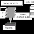 Scanning probe microscope Current state and development of scanning probe microscopy