Coursework: Scanning probe microscopy. Scanning probe microscope Current state and development of scanning probe microscopy
Introduction
At present, the scientific and technical direction - nanotechnology - is rapidly developing, covering a wide range of both fundamental and applied research. This is a fundamentally new technology that can solve problems in such diverse areas as communications, biotechnology, microelectronics and energy. Today, more than a hundred young companies are developing nanotechnology products that will enter the market in the next two to three years.
Nanotechnologies will become the leading technologies in the 21st century and will contribute to the development of the economy and the social sphere of society, they can become a prerequisite for a new industrial revolution. In the previous two hundred years, progress in the industrial revolution was achieved at the cost of about 80% of the earth's resources. Nanotechnologies will significantly reduce the volume of resource consumption and will not put pressure on the environment, they will play a leading role in the life of mankind, as, for example, the computer has become an integral part of people's lives.
Progress in nanotechnology was stimulated by the development of experimental methods of research, the most informative of which are the methods of scanning probe microscopy, the invention and distribution of which the world owes in particular to the Nobel laureates of 1986 - Professor Heinrich Rohrer and Dr. Gerd Binnig.
The world was fascinated by the discovery of such simple methods for visualizing atoms, and even with the ability to manipulate them. Many research groups began to design home-made devices and experiment in this direction. As a result, a number of convenient device schemes were born, various methods for visualizing the results of the probe-surface interaction were proposed, such as: lateral force microscopy, magnetic force microscopy, microscopy for recording magnetic, electrostatic, and electromagnetic interactions. Methods of near-field optical microscopy have been intensively developed. Methods have been developed for directed, controlled action in the probe-surface system, for example, nanolithography - changes occur on the surface under the influence of electrical, magnetic influences, plastic deformations, and light in the probe-surface system. Technologies were created for the production of probes with specified geometric parameters, with special coatings and structures for visualizing various surface properties.
Scanning probe microscopy (SPM) is one of the powerful modern methods for studying the morphology and local properties of a solid surface with high spatial resolution. Over the past 10 years, scanning probe microscopy has evolved from an exotic technique accessible only to a limited number of research groups into a widely used and successfully used tool for studying surface properties. At present, almost no research in the field of surface physics and thin-film technologies is complete without the use of SPM methods. The development of scanning probe microscopy also served as the basis for the development of new methods in nanotechnology - the technology for creating structures with nanometer scales.
1. Historical background
To observe small objects, the Dutchman Anthony van Leeuwenhoek invented the microscope in the 17th century, discovering the world of microbes. His microscopes were imperfect and gave magnifications from 150 to 300 times. But his followers improved this optical device, laying the foundation for many discoveries in biology, geology, and physics. However, at the end of the 19th century (1872), the German optician Ernst Karl Abbe showed that due to the diffraction of light, the resolution of the microscope (that is, the minimum distance between objects when they do not yet merge into one image) is limited by the wavelength of light (0.4 - 0.8 µm). Thus, he saved a lot of efforts of opticians who were trying to make more advanced microscopes, but disappointed biologists and geologists who lost hope of obtaining an instrument with a magnification above 1500x.
The history of the creation of the electron microscope is a wonderful example of how independently developing fields of science and technology can, by exchanging the information received and joining efforts, create a new powerful tool for scientific research. The pinnacle of classical physics was the theory of the electromagnetic field, which explained the propagation of light, the emergence of electric and magnetic fields, the movement of charged particles in these fields as the propagation of electromagnetic waves. Wave optics made clear the phenomenon of diffraction, the mechanism of image formation and the play of factors that determine resolution in a light microscope. We owe successes in the field of theoretical and experimental physics to the discovery of the electron with its specific properties. These separate and seemingly independent developments led to the creation of the foundations of electron optics, one of the most important applications of which was the invention of the EM in the 1930s. A direct hint of this possibility can be considered the hypothesis of the wave nature of the electron, put forward in 1924 by Louis de Broglie and experimentally confirmed in 1927 by K. Davisson and L. Germer in the USA and J. Thomson in England. Thus, an analogy was suggested, which made it possible to construct an EM according to the laws of wave optics. H. Bush discovered that electronic images can be formed using electric and magnetic fields. In the first two decades of the 20th century the necessary technical prerequisites were also created. Industrial laboratories working on a cathode-ray oscilloscope provided vacuum technology, stable sources of high voltage and current, and good electron emitters.
In 1931 R. Rudenberg filed a patent application for a transmission electron microscope, and in 1932 M. Knoll and E. Ruska built the first such microscope, using magnetic lenses to focus electrons. This instrument was the forerunner of the modern optical transmission electron microscope (OTEM). (Ruska was rewarded for his work by winning the 1986 Nobel Prize in Physics.) In 1938 Ruska and B. von Borries built a prototype industrial OPEM for Siemens-Halske in Germany; this instrument eventually made it possible to achieve a resolution of 100 nm. A few years later, A. Prebus and J. Hiller built the first high-resolution OPEM at the University of Toronto (Canada).
The wide possibilities of OPEM became apparent almost immediately. Its industrial production was started simultaneously by Siemens-Halske in Germany and RCA Corporation in the USA. In the late 1940s, other companies began to produce such devices.
The SEM in its current form was invented in 1952 by Charles Otley. True, preliminary versions of such a device were built by Knoll in Germany in the 1930s and by Zworykin with employees at the RCA corporation in the 1940s, but only the Otley device could serve as the basis for a number of technical improvements that culminated in the introduction of an industrial version of the SEM into production in the middle 1960s. The circle of consumers of such a rather easy-to-use device with a three-dimensional image and an electronic output signal has expanded with the speed of an explosion. At present, there are a good dozen industrial SEM manufacturers on three continents and tens of thousands of such devices used in laboratories around the world. In the 1960s, ultrahigh-voltage microscopes were developed to study thicker samples. , where a device with an accelerating voltage of 3.5 million volts was put into operation in 1970. RTM was invented by G. Binnig and G. Rohrer in Zurich in 1979. This very simple device provides atomic resolution of surfaces. Binnig and Rohrer (simultaneously with Ruska) received the Nobel Prize for the creation of the RTM.
The scanning probe microscope was invented in 1986 by Rohrer and Binnig. Since its invention, STM has been widely used by scientists of various specialties, covering almost all natural science disciplines, from fundamental research in physics, chemistry, biology, to specific technological applications. The principle of operation of the STM is so simple, and the potential possibilities are so great that it is impossible to predict its impact on science and technology even in the near future.
As it turned out later, almost any interaction of the tip probe with the surface (mechanical, magnetic) can be converted into an image of the surface with the help of appropriate instruments and computer programs.
The installation of a scanning probe microscope consists of several functional blocks shown in Fig. 1. This is, firstly, the microscope itself with a piezomanipulator for controlling the probe, a tunnel current-to-voltage converter, and a stepper motor for sample supply; block of analog-to-digital and digital-to-analog converters and high-voltage amplifiers; stepper motor control unit; a board with a signal processor that calculates the feedback signal; a computer that collects information and provides a user interface. Structurally, the DAC and ADC unit is installed in the same housing with the stepper motor control unit. The board with the signal processor (DSP - Digital Signal Processor) ADSP 2171 from Analog Devices is installed in the ISA expansion slot of a personal computer.
A general view of the mechanical system of the microscope is shown in fig. 2. The mechanical system includes a base with a piezomanipulator and a smooth sample feed system on a stepper motor with a gearbox and two removable measuring heads for operation in scanning tunneling and atomic force microscopy modes. The microscope makes it possible to obtain stable atomic resolution on traditional test surfaces without the use of additional seismic and acoustic filters.
2. Operating principles of scanning probe microscopes
In scanning probe microscopes, the study of the surface microrelief and its local properties is carried out using specially prepared probes in the form of needles. The working part of such probes (the tip) is about ten nanometers in size. The characteristic distance between the probe and the sample surface in probe microscopes is 0.1 – 10 nm in order of magnitude. The operation of probe microscopes is based on various types of interaction between the probe and the surface. Thus, the operation of a tunneling microscope is based on the phenomenon of tunneling current flowing between a metal needle and a conducting sample; different types of force interaction underlie the operation of atomic force, magnetic force and electric force microscopes. Let us consider the common features inherent in various probe microscopes. Let the interaction of the probe with the surface be characterized by some parameter P. If there is a sufficiently sharp and one-to-one dependence of the parameter P on the probe-sample distance, then this parameter can be used to organize a feedback system (FS) that controls the distance between the probe and the sample. On fig. 3 schematically shows the general principle of SPM feedback organization.
The feedback system maintains the value of the parameter Р constant, equal to the value specified by the operator. If the probe-surface distance changes, then the parameter P changes. In the OS system, a difference signal is generated that is proportional to the value ΔP = P - P, which is amplified to the desired value and fed to the actuating element of the IE. The actuating element processes this difference signal by moving the probe closer to the surface or moving it away until the difference signal becomes zero. in this way, the probe-sample distance can be maintained with great accuracy. When the probe moves along the sample surface, the interaction parameter P changes due to the surface topography. The OS system works out these changes, so that when the probe moves in the X, Y plane, the signal on the actuating element turns out to be proportional to the surface topography. To obtain an SPM image, a specially organized process of scanning a sample is carried out. When scanning, the probe first moves over the sample along a certain line (line scan), while the signal value on the actuating element, proportional to the surface topography, is recorded in the computer memory. Then the probe returns to the starting point and goes to the next scan line (frame scan), and the process is repeated again. The feedback signal recorded in this way during scanning is processed by a computer, and then the SPM image of the surface topography is constructed using computer graphics. Along with the study of the surface topography, probe microscopes make it possible to study various surface properties: mechanical, electrical, magnetic, optical, and others.
3. Scanning elements (scanners) of probe microscopes
3.1 Scanning elements
To operate probe microscopes, it is necessary to control the probe-sample working distance and move the probe in the sample plane with high accuracy (at the level of fractions of an angstrom). This problem is solved with the help of special manipulators - scanning elements (scanners). The scanning elements of probe microscopes are made of piezoelectrics, materials with piezoelectric properties. Piezoelectrics change their dimensions in an external electric field. The equation for the inverse piezoelectric effect for crystals is written as:
where u is the strain tensor, E are the components of the electric field, and d are the components of the piezoelectric coefficient tensor. The form of the piezoelectric coefficient tensor is determined by the type of crystal symmetry.
In various technical applications, transducers made of piezoceramic materials are widely used. Piezoceramics is a polarized polycrystalline material obtained by sintering powders from crystalline ferroelectrics. Polarization of ceramics is carried out as follows. Ceramics are heated above the Curie temperature (for most piezoceramics, this temperature is less than 300C), and then slowly cooled in a strong (about 3 kV/cm) electric field. After cooling, the piezoceramic has induced polarization and acquires the ability to change its dimensions (increase or decrease depending on the mutual direction of the polarization vector and the vector of the external electric field).
Tubular piezoelectric elements are widely used in scanning probe microscopy (Fig. 4). They make it possible to obtain sufficiently large displacements of objects at relatively small control voltages. Tubular piezoelectric elements are hollow thin-walled cylinders made of piezoceramic materials. Typically, electrodes in the form of thin metal layers are deposited on the outer and inner surfaces of the tube, while the ends of the tube remain uncoated.
Under the influence of the potential difference between the inner and outer electrodes, the tube changes its longitudinal dimensions. In this case, the longitudinal deformation under the action of a radial electric field can be written as:
where l is the length of the tube in the undeformed state. The absolute elongation of the piezotube is
where h is the wall thickness of the piezotube, V is the potential difference between the inner and outer electrodes. Thus, at the same voltage V, the elongation of the tube will be the greater, the greater its length and the smaller its wall thickness.
The connection of three tubes into one node allows organizing precision movements of the microscope probe in three mutually perpendicular directions. Such a scanning element is called a tripod.
The disadvantages of such a scanner are the complexity of manufacturing and the strong asymmetry of the design. To date, scanners based on a single tubular element are most widely used in scanning probe microscopy. The general view of the tubular scanner and the layout of the electrodes are shown in fig. 5. The material of the tube has a radial direction of the polarization vector.
The inner electrode is usually solid. The outer electrode of the scanner is divided along the generatrices of the cylinder into four sections. When antiphase voltages are applied to opposite sections of the outer electrode (relative to the inner one), the tube section contracts in the place where the field direction coincides with the polarization direction, and elongation occurs where they are directed in opposite directions. This causes the tube to bend in the appropriate direction. Thus, scanning is carried out in the X, Y plane. A change in the potential of the internal electrode relative to all external sections leads to an elongation or contraction of the tube along the Z axis. Thus, it is possible to organize a three-coordinate scanner based on a single piezotube. Real scanning elements often have a more complex design, but the principles of their operation remain the same.
Scanners based on bimorph piezoelectric elements are also widely used. A bimorph is two piezoelectric plates glued together in such a way that the polarization vectors in each of them are directed in opposite directions (Fig. 6). If voltage is applied to the bimorph electrodes, as shown in Fig. 6, then one of the plates will expand and the other will shrink, which will lead to the bending of the entire element. In real designs of bimorph elements, a potential difference is created between the internal common and external electrodes so that in one element the field coincides with the direction of the polarization vector, and in the other it is directed oppositely.
Bimorph bending under the action of electric fields is the basis for the operation of bimorph piezoscanners. By combining three bimorph elements in one construction, it is possible to implement a tripod on bimorph elements.
If the outer electrodes of the bimorph element are divided into four sectors, then it is possible to organize the movement of the probe along the Z axis and in the X, Y plane on one bimorph element (Fig. 7).
Indeed, by applying antiphase voltages to opposite pairs of sections of external electrodes, it is possible to bend the bimorph so that the probe will move in the X, Y plane (Fig. 7 (a, b)). And by changing the potential of the inner electrode relative to all sections of the outer electrodes, it is possible to bend the bimorph by moving the probe in the Z direction (Fig. 7 (c, d)).
3.2 Non-linearity of piezoceramics
Despite a number of technological advantages over crystals, piezoceramics have some disadvantages that adversely affect the operation of scanning elements. One such drawback is the non-linearity of the piezoelectric properties. On fig. 8, as an example, the dependence of the displacement of the piezotube in the Z direction on the magnitude of the applied field is shown. In the general case (especially at high control fields), piezoceramics are characterized by a nonlinear dependence of deformations on the field (or on the control voltage).
Thus, the deformation of a piezoceramic is a complex function of an external electric field:
For small control fields, this dependence can be represented in the following form:
u = d* E+ α* E*E+…
where d and α are linear and quadratic modules of the piezoelectric effect.
Typical values of the fields E, at which nonlinear effects begin to show, are on the order of 100 V/mm. Therefore, for the correct operation of scanning elements, control fields are usually used in the linearity region of ceramics (E< Е) .
scanning probe electron microscope
3.3 Piezo ceramic creep and piezo ceramic hysteresis
Another disadvantage of piezoceramics is the so-called creep (creep - creep) - a delay in the response to a change in the magnitude of the control electric field.
Creep leads to geometric distortions associated with this effect in SPM images. The creep is especially strong when the scanners are brought to a given point for local measurements and at the initial stages of the scanning process. To reduce the effect of ceramic creep, time delays are applied in these processes, which allow partially compensating for the scanner's delay.
Another disadvantage of piezoceramics is the ambiguity of the dependence of elongation on the direction of change in the electric field (hysteresis).
This leads to the fact that, at the same control voltages, the piezoceramic is at different points of the trajectory, depending on the direction of motion. To exclude distortions of SPM images due to the hysteresis of piezoceramics, information is recorded when scanning samples only on one of the branches of the dependence .
4. Devices for precision movement of the probe and sample
4.1 Mechanical gearboxes
One of the important technical problems in scanning probe microscopy is the need for precise movement of the probe and sample in order to form the working gap of the microscope and select the area of the surface to be studied. To solve this problem, various types of devices are used that move objects with high accuracy. Various mechanical gearboxes are widely used, in which the coarse movement of the initial mover corresponds to the fine movement of the object being displaced. Ways to reduce displacements can be different. Lever devices are widely used, in which the reduction of the amount of movement is carried out due to the difference in the length of the arms of the levers. The scheme of the lever gearbox is shown in fig. 9.
The mechanical lever makes it possible to obtain a displacement reduction with a coefficient
Thus, the greater the ratio of the arm L to the arm l, the more accurately it is possible to control the process of approaching the probe and the sample.
Also, in the designs of microscopes, mechanical gearboxes are widely used, in which the reduction of displacements is achieved due to the difference in the stiffness coefficients of two elastic elements connected in series (Fig. 10). The design consists of a rigid base, a spring and an elastic beam. The stiffness of the spring k and the elastic beam K are selected in such a way that the following condition is fulfilled: k< K .
The reduction factor is equal to the ratio of the stiffness coefficients of the elastic elements:
Thus, the greater the ratio of the beam stiffness to the spring stiffness, the more precisely the displacement of the working element of the microscope can be controlled.
4.2 Stepper motors
Stepper motors (SHED) are electromechanical devices that convert electrical impulses into discrete mechanical movements. An important advantage of stepper motors is that they provide an unambiguous dependence of the rotor position on the input current pulses, so that the angle of rotation of the rotor is determined by the number of control pulses. In the SHED, the torque is generated by the magnetic fluxes generated by the stator and rotor poles, which are appropriately oriented relative to each other.
The simplest designs are permanent magnet motors. They consist of a stator which has windings and a rotor containing permanent magnets. On fig. 11 shows a simplified design of a stepper motor.
The alternating poles of the rotor have a rectilinear shape and are parallel to the axis of the motor. The motor shown in the figure has 3 pairs of rotor poles and 2 pairs of stator poles. The motor has 2 independent windings, each of which is wound on two opposite poles of the stator. the motor shown has a step size of 30 deg. When the current is turned on in one of the windings, the rotor tends to take a position in which the opposite poles of the rotor and stator are opposite each other. For continuous rotation, you need to turn on the windings alternately.
In practice, stepper motors are used, which have a more complex design and provide from 100 to 400 steps per revolution of the rotor. If such an engine is paired with a threaded connection, then with a thread pitch of about 0.1 mm, an object positioning accuracy of about 0.25 - 1 micron is ensured. To increase the accuracy, additional mechanical gearboxes are used. Possibility of electrical control makes it possible to effectively use the SHED in automated systems for approaching the probe and the sample of scanning probe microscopes.
4.3 Piezo stepper motors
The requirements for good isolation of devices from external vibrations and the need to operate probe microscopes in vacuum conditions impose serious restrictions on the use of purely mechanical devices for moving the probe and sample. In this regard, devices based on piezoelectric transducers, which allow remote control of the movement of objects, are widely used in probe microscopes.
One of the designs of a stepper inertial piezoelectric motor is shown in fig. 12. This device contains a base (1) on which a piezoelectric tube (2) is fixed. The tube has electrodes (3) on the outer and inner surfaces. At the end of the tube, a split spring (4) is fixed, which is a cylinder with separate springy petals. The object holder (5) is installed in the spring - a rather massive cylinder with a polished surface. The object to be moved can be attached to the holder with a spring or a union nut, which allows the device to work in any orientation in space.
The device works as follows. To move the object holder in the direction of the Z axis, a sawtooth pulsed voltage is applied to the electrodes of the piezotube (Fig. 13).
On the flat edge of the sawtooth voltage, the tube smoothly lengthens or contracts depending on the polarity of the voltage, and its end, together with the spring and the object holder, is displaced by the distance:
At the moment the sawtooth voltage is released, the tube returns to its original position with acceleration a, which initially has a maximum value:
where ω is the resonant frequency of longitudinal oscillations of the tube. When condition F< ma (m – масса держателя объекта, F - сила трения между держателем объекта и разрезной пружиной), держатель объекта, в силу своей инерционности, проскальзывает относительно разрезной пружины. В результате держатель объекта перемещается на некоторый шаг К Δl относительно исходного положения. Коэффициент К определяется соотношением масс деталей конструкции и жесткостью разрезной пружины. При смене полярности импульсов управляющего напряжения происходит изменение направления движения объекта. Таким образом, подавая пилообразные напряжения различной полярности на электроды пьезотрубки, можно перемещать объект в пространстве и производить сближение зонда и образца в сканирующем зондовом микроскопе .
5. Protection of probe microscopes from external influences
5.1 Vibration protection
To protect devices from external vibrations, various types of vibration isolation systems are used. Conventionally, they can be divided into passive and active. The main idea behind passive vibration isolation systems is as follows. The amplitude of the forced oscillations of a mechanical system quickly decreases with an increase in the difference between the frequency of the exciting force and the natural resonant frequency of the system (a typical amplitude-frequency characteristic (AFC) of an oscillatory system is shown in Fig. 14).
Therefore, external influences with frequencies ω > ω have practically no noticeable effect on the oscillatory system. Therefore, if the measuring head of a probe microscope is placed on a vibration-isolating platform or on an elastic suspension (Fig. 15), then only external oscillations with frequencies close to the resonant frequency of the vibration-isolating system will pass to the microscope body. Since the natural frequencies of the SPM heads are 10–100 kHz, by choosing the resonant frequency of the vibration isolation system sufficiently low (of the order of 5–10 Hz), it is possible to effectively protect the device from external vibrations. In order to dampen oscillations at natural resonant frequencies, dissipative elements with viscous friction are introduced into vibration isolating systems.
Thus, in order to provide effective protection, it is necessary that the resonant frequency of the vibration isolation system be as low as possible. However, it is difficult to realize very low frequencies in practice.
Active systems for suppressing external vibrations are successfully used to protect SPM heads. Such devices are electromechanical systems with negative feedback, which ensures a stable position of the vibration isolating platform in space (Fig. 16) .
5.2 Protection against acoustic noise
Another source of vibration of structural elements of probe microscopes is acoustic noise of various nature.
A feature of acoustic interference is that acoustic waves directly affect the structural elements of the SPM heads, which leads to vibrations of the probe relative to the surface of the sample under study. To protect the SPM from acoustic interference, various protective caps are used to significantly reduce the level of acoustic interference in the region of the working gap of the microscope. The most effective protection against acoustic interference is to place the measuring head of the probe microscope in a vacuum chamber (Fig. 17) .
5.3 Stabilization of the thermal drift of the position of the probe above the surface
One of the important problems of SPM is the problem of stabilization of the position of the probe over the surface of the sample under study. The main source of instability of the probe position is a change in the ambient temperature or heating of the structural elements of the probe microscope during its operation. A change in the temperature of a solid leads to the appearance of thermoelastic deformations. Such deformations have a very significant effect on the operation of probe microscopes. To reduce thermal drift, temperature control of the SPM measuring heads is used or thermal compensating elements are introduced into the design of the heads. The idea of thermal compensation is as follows. Any SPM design can be represented as a set of elements with different thermal expansion coefficients (Fig. 18 (a)).
To compensate for thermal drift, compensating elements with different expansion coefficients are introduced into the design of the SPM measuring heads, so that the condition that the sum of thermal expansions in the various arms of the structure is equal to zero is satisfied:
ΔL = ∑ ΔL = ΔT ∑αl0
The simplest way to reduce the thermal drift of the probe position along the Z axis is to introduce compensating elements made of the same material and with the same characteristic dimensions as the main structural elements into the SPM design (Fig. 18 (b)). When the temperature of this design changes, the displacement of the probe in the Z direction will be minimal. To stabilize the position of the probe in the X, Y plane, the measuring heads of microscopes are made in the form of axially symmetrical structures.
6. Formation and processing of SPM images
6.1 Scan process
The process of surface scanning in a scanning probe microscope is similar to the movement of an electron beam across a screen in a TV cathode ray tube. The probe moves along the line (line), first in the forward and then in the opposite direction (line scan), and then moves to the next line (frame scan) (Fig. 19). The movement of the probe is carried out with the help of a scanner in small steps under the action of sawtooth voltages generated by digital-to-analog converters. Registration of information about the surface topography is performed, as a rule, on a straight pass.
The information obtained using a scanning probe microscope is stored as an SPM frame - a two-dimensional array of integers a (matrix). The physical meaning of these numbers is determined by the value that was digitized during the scanning process. Each value of the pair of indices ij corresponds to a certain point of the surface within the scanning field. The coordinates of the surface points are calculated by simply multiplying the corresponding index by the distance between the points at which information was recorded.
As a rule, SPM frames are square matrices having a size of 2 (mainly 256x256 and 512x512 elements). Visualization of SPM frames is performed by means of computer graphics, mainly in the form of three-dimensional (3D) and two-dimensional brightness (2D) images. In 3D visualization, the image of a surface is built in an axonometric perspective using pixels or lines. In addition to this, various methods of highlighting pixels corresponding to different heights of the surface relief are used. The most effective way to colorize 3D images is to simulate the conditions of surface illumination by a point source located at some point in space above the surface (Fig. 20). In this case, it is possible to emphasize small-scale unevenness of the relief. Also, by means of computer processing and graphics, scaling and rotation of 3D SPM images are implemented. In 2D rendering, each point on a surface is assigned a color. The most widely used are gradient palettes, in which the coloring of the image is done with a tone of a certain color in accordance with the height of a surface point.
Local SPM measurements, as a rule, are associated with the registration of the dependences of the quantities under study on various parameters. For example, these are the dependences of the magnitude of the electric current through the probe-surface contact on the applied voltage, the dependences of various parameters of the force interaction between the probe and the surface on the probe-sample distance, etc. This information is stored in the form of vector arrays or in the form of 2 x N matrices. For their visualization The microscope software provides a set of standard tools for displaying function graphs.
6.2 Methods for constructing and processing images
When studying the properties of objects using scanning probe microscopy, the main result of scientific research is, as a rule, three-dimensional images of the surface of these objects. The adequacy of the interpretation of images depends on the qualifications of the specialist. At the same time, when processing and building images, a number of traditional techniques are used, which you should be aware of when analyzing images. Scanning probe microscope appeared at the time of intensive development of computer technology. Therefore, when recording three-dimensional images, it used digital information storage methods developed for computers. This resulted in significant convenience in image analysis and processing, but the photographic quality inherent in electron microscopy methods had to be sacrificed. Information obtained using a probe microscope is represented in a computer in the form of a two-dimensional matrix of integers. Each number in this matrix, depending on the scan mode, can be the value of the tunnel current, or the value of the deflection, or the value of some more complex function. If you show this matrix to a person, then he will not be able to get any coherent idea of the surface under study. So, the first problem is to convert the numbers into a readable form. This is done in the following way. The numbers in the original matrix lie in a certain range, there are minimum and maximum values. This range of integers is assigned a color palette. Thus, each value of the matrix is mapped to a point of a certain color on a rectangular image. The row and column containing this value become the coordinates of the point. As a result, we get a picture in which, for example, the height of the surface is conveyed in color - as on a geographical map. But on the map, only dozens of colors are usually used, and in our picture there are hundreds and thousands of them. For ease of perception, points that are close in height should be transmitted in similar colors. It may turn out, and as a rule it always does, that the range of initial values is greater than the number of possible colors. In this case, there is a loss of information, and an increase in the number of colors is not a way out, since the capabilities of the human eye are limited. Additional processing of information is required, and depending on the tasks, the processing should be different. Some people need to see the whole picture, while others want to see the details. Various methods are used for this.
6.3 Subtraction of constant slope
Surface images taken with probe microscopes tend to have a general slope. This may be due to several reasons. First, the slope may appear due to inaccurate positioning of the sample relative to the probe; secondly, it can be associated with temperature drift, which leads to a displacement of the probe relative to the sample; thirdly, it may be due to the nonlinearity of the piezoscanner movements. A large amount of usable space in the SPM frame is spent on displaying the tilt, so small image details become invisible. To eliminate this disadvantage, the operation of subtracting the constant slope is performed. To do this, at the first stage, the approximating plane is found by the least squares method
Р(х,y), which has minimal deviations from the surface topography Z = f(x,y), then this plane is subtracted from the SPM image. It is expedient to carry out the subtraction in different ways, depending on the nature of the slope.
If the tilt in the SPM image is due to the tilt of the sample relative to the probe sample, then it is advisable to rotate the plane by an angle corresponding to the angle between the normal to the plane and the Z axis; in this case, the coordinates of the surface Z = f(x,y) are transformed in accordance with the transformations of the spatial rotation. However, with this transformation, it is possible to obtain an image of the surface in the form of a multivalued function Z = f(x, y). If the slope is due to thermal drift, then the procedure for subtracting the slope is reduced to subtracting the Z - coordinates of the plane from the Z - coordinates of the SPM image:
The result is an array with a smaller range of values, and fine details in the image will be reflected in more colors, becoming more visible.
6.4 Elimination of distortions associated with non-ideal scanner
The imperfection of the scanner properties leads to the fact that the SPM image contains a number of specific distortions. Some of the non-idealities of the scanner, such as uneven forward and reverse strokes of the scanner (hysteresis), creep and non-linearity of the piezoceramics are compensated by hardware and the choice of optimal scanning modes. However, despite this, SPM images contain distortions that are difficult to eliminate at the hardware level. In particular, since the movement of the scanner in the plane of the sample affects the position of the probe above the surface, SPM images are a superposition of the real relief and some surface of the second (and often higher) order.
To eliminate this kind of distortion, the least squares method is used to find an approximating second-order surface Р(x,y), which has minimal deviations from the original function Z = f(x,y), and then this surface is subtracted from the original SPM image:
Another type of distortion is associated with the non-linearity and non-orthogonality of scanner movements in the X, Y plane. This leads to a distortion of geometric proportions in various parts of the SPM image of the surface. To eliminate such distortions, the procedure for correcting SPM images is performed using a file of correction coefficients, which is created when scanning test structures with a well-known relief by a specific scanner.
6.5 Filtering SPM images
Equipment noise (mainly the noise of highly sensitive input amplifiers), probe-sample contact instability during scanning, external acoustic noise and vibrations lead to the fact that SPM images, along with useful information, have a noise component. Partially the noise of SPM images can be removed by software.
6.6 Median filtering
Good results in removing high-frequency random noise in SPM frames are obtained by median filtering. This is a non-linear image processing method, the essence of which can be explained as follows. A working filter window is selected, consisting of nxn points (for definiteness, we take a 3 x 3 window, i.e. containing 9 points (Fig. 24)).
In the process of filtering, this window moves across the frame from point to point, and the following procedure is performed. The amplitude values of the SPM image at the points of this window are arranged in ascending order, and the value in the center of the sorted row is placed in the center point of the window. Then the window is shifted to the next point, and the sorting procedure is repeated. Thus, powerful random outliers and dips in such sorting always end up on the edge of the sorted array and will not be included in the final (filtered) image. With this processing, unfiltered areas remain at the edges of the frame, which are discarded in the final image.
6.7 Methods for restoring a surface from its SPM image
One of the disadvantages inherent in all methods of scanning probe microscopy is the finite size of the working part of the probes used. This leads to a significant deterioration in the spatial resolution of microscopes and significant distortions in SPM images when scanning surfaces with relief irregularities comparable to the characteristic dimensions of the working part of the probe.
In fact, the image obtained in the SPM is a "convolution" of the probe and the surface under study. The process of “convolution” of the probe shape with the surface relief is illustrated in the one-dimensional case in Fig. 25.
Partially, this problem can be solved by recently developed methods for reconstructing SPM images, based on computer processing of SPM data, taking into account the specific shape of the probes. The most effective method of surface reconstruction is the numerical deconvolution method, which uses the shape of the probe obtained experimentally when scanning test (with a well-known surface topography) structures.
It should be noted that complete restoration of the sample surface is possible only if two conditions are met: the probe touched all points of the surface during scanning, and at each moment the probe touched only one point of the surface. If the probe cannot reach some areas of the surface during scanning (for example, if the sample has overhanging sections of the relief), then only a partial restoration of the relief occurs. Moreover, the greater the number of surface points touched by the probe during scanning, the more reliably the surface can be reconstructed.
In practice, the SPM image and the experimentally determined shape of the probe are two-dimensional arrays of discrete values, for which the derivative is a poorly defined quantity. Therefore, instead of calculating the derivative of discrete functions in practice, in the numerical deconvolution of SPM images, the condition of the minimum distance between the probe and the surface is used when scanning with a constant average height .
In this case, the height of the surface relief at a given point can be taken as the minimum distance between the probe point and the corresponding surface point for a given position of the probe relative to the surface. In its physical meaning, this condition is equivalent to the condition of equality of derivatives, however, it allows one to search for the points of contact of the probe with the surface by a more adequate method, which significantly reduces the time of relief reconstruction.
To calibrate and determine the shape of the working part of the probes, special test structures with known parameters of the surface relief are used. The types of the most common test structures and their characteristic images obtained using an atomic force microscope are shown in fig. 26 and fig. 27 .
The spiky scaling grid allows for a good alignment of the probe tip, while the rectangular grid helps to reshape the side surface. By combining the results of scanning these gratings, it is possible to completely restore the shape of the working part of the probes.
7. Modern SPM
1) Scanning probe microscope SM-300
Designed to study the morphological features and structure of the pore space. The SM-300 (Figure 28) has a built-in optical positioning microscope that eliminates the need to endlessly search for an area of interest. A color optical image of the sample, with a slight increase, is displayed on a computer monitor. The crosshair on the optical image corresponds to the position of the electron beam. Using crosshairs, quick positioning can be done to define the area of interest for raster analysis.
Rice. 28. SPM SM-300 electron microscope. The optical positioning unit is equipped with a separate computer, which ensures its hardware independence from the scanning microscope.
SM-300 CAPABILITIES
Guaranteed 4 nm resolution
Unique optical positioning microscope (optional)
· Intuitive Windows® software
Fully computer controlled scanning microscope and imaging
Standard TV output with digital signal processing
Computer control of the low vacuum system (option)
All studies are performed at the same position of the applicate axis (12 mm)
Elemental X-ray microanalysis in low and high vacuum modes (optional)
Ability to work in normal room lighting conditions
Investigation of non-conductive samples without their preliminary preparation
5.5 nm resolution in low vacuum mode
Software control of switching modes
Selectable chamber vacuum range 1.3 – 260 Pa
Displaying an image on a computer monitor
Serial V-backscattered Robinson sensor
2) Supra50VP high resolution scanning probe microscope with INCA Energy+Oxford microanalysis system.
The device (Fig. 29) is intended for research in all areas of materials science, in the field of nano- and biotechnologies. The instrument handles large sample sizes, and it also supports variable pressure operation for testing non-conductive samples without preparation. Rice. 29. SPM Supra50VP
PARAMETERS:
Accelerating voltage 100 V - 30 kV (field emission cathode)
Max. magnification up to x 900000
Ultra high resolution - up to 1 nm (at 20 kV)
Vacuum mode with variable pressure from 2 to 133 Pa
Accelerating voltage - from 0.1 to 30 kV
Motorized stage with five degrees of freedom
EDX detector resolution 129 eV on the Ka(Mn) line, counting rate up to 100,000 pulses/s
3) LEO SUPRA 25 modernized microscope with "GEMINI" column and field emission (Fig.30).
– Designed for nanoanalysis research
– Can be connected to both EDX and WDX systems for microanalysis
– Resolution 1.5 nm at 20 kV, 2 nm at 1 kV.
Conclusion
Over the past years, the use of probe microscopy has made it possible to achieve unique scientific results in various fields of physics, chemistry and biology.
If the first scanning probe microscopes were indicators for qualitative research, then the modern scanning probe microscope is a device that integrates up to 50 different research methods. It is capable of performing specified displacements in the probe-sample system with an accuracy of 0.1%, calculating the probe form factor, performing precision measurements of sufficiently large sizes (up to 200 µm in the scanning plane and 15–20 µm in height) and, at the same time, provide submolecular resolution.
Scanning probe microscopes have become one of the most demanded classes of instruments for scientific research on the world market. New instrument designs are constantly being created, specialized for various applications.
The dynamic development of nanotechnology requires more and more expansion of the capabilities of research technology. High-tech companies around the world are working on the creation of research and technological nanocomplexes that combine entire groups of analytical methods, such as Raman spectroscopy, luminescence spectroscopy, X-ray spectroscopy for elemental analysis, high-resolution optical microscopy, electron microscopy, focused ion beams. Systems acquire powerful intellectual capabilities: the ability to recognize and classify images, highlight the required contrasts, are endowed with the ability to model results, and computing power is provided by the use of supercomputers.
The developed technique has powerful possibilities, but the ultimate goal of its use is to obtain scientific results. Mastering the capabilities of this technique is in itself a task of a high degree of complexity, requiring the training of highly qualified specialists who are able to effectively use these devices and systems.
Bibliography
1. Nevolin V. K. Fundamentals of tunnel-probe technology / V. K. Nevolin, - M .: Nauka, 1996, - 91 p.
2. Kulakov Yu. A. Electron microscopy / Yu. A. Kulakov, - M.: Knowledge, 1981, - 64 p.
3. Volodin A.P. Scanning microscopy / A. P. Volodin, - M .: Nauka, 1998, - 114 p.
4. Scanning probe microscopy of biopolymers / Edited by I. V. Yaminsky, - M.: Nauchny Mir, 1997, - 86 p.
5. Mironov V. Fundamentals of scanning probe microscopy / V. Mironov, - M.: Technosfera, 2004, - 143 p.
6. Rykov S. A. Scanning probe microscopy of semiconductor materials / S. A. Rykov, St. Petersburg: Nauka, 2001, 53 p.
7. Bykov V. A., Lazarev M. I. Scanning probe microscopy for science and industry / V. A. Bykov, M. I. Lazarev // Electronics: science, technology, business, - 1997, - No. 5, - With. 7 - 14.
7. Application of a scanning probe microscope for the study of biological objects
7. Application of a scanning probe microscope for the study of biological objects 1
7.1. Goals of work 2
7.2. Information for the teacher 3
7.4. Guidelines 31
7.5. Safety 32
7.6. Task 32
7.7. Security questions 32
7.8. Literature 32
Laboratory work was developed by the Nizhny Novgorod State University. N.I. Lobachevsky
7.1. Goals of the work
The study of the morphological parameters of biological structures is an important task for biologists, since the size and shape of some structures largely determine their physiological properties. Comparing morphological data with functional characteristics, one can obtain complete information about the participation of living cells in maintaining the physiological balance of the human or animal body.
Previously, biologists and physicians had the opportunity to study their preparations only on optical and electron microscopes. These studies gave some picture of the morphology of cells fixed, stained and with thin metal coatings obtained by sputtering. It was not possible to study the morphology of living objects, its changes under the influence of various factors, but it was very tempting.
Scanning probe microscopy (SPM) has opened up new possibilities in the study of cells, bacteria, biological molecules, DNA under conditions as close as possible to native ones. SPM allows you to study biological objects without special fixatives and dyes, in air, or even in a liquid medium.
Currently, SPM is used in a wide variety of disciplines, both in fundamental scientific research and in applied high-tech developments. Many research institutes of the country are equipped with probe microscopy equipment. In this regard, the demand for highly qualified specialists is constantly growing. To meet this requirement, NT-MDT (Zelenograd, Russia) has developed a specialized educational and scientific laboratory for scanning probe microscopy NanoEducator.
SPM NanoEducator specially designed for students to conduct laboratory work. This device is aimed at a student audience: it is fully controlled by a computer, has a simple and intuitive interface, animation support, involves the gradual development of techniques, the absence of complex settings and inexpensive consumables.
In this laboratory work, you will learn about scanning probe microscopy, get acquainted with its basics, study the design and principles of the educational SPM NanoEducator, learn how to prepare biological preparations for research, get your first SPM image of a complex of lactic acid bacteria and learn the basics of processing and presenting measurement results.
7.2 Information for teacher 1
Laboratory work is carried out in several stages:
1. Sample preparation is done by each student individually.
2. Obtaining the first image is carried out on one device under the supervision of a teacher, then each student examines his sample independently.
3. The processing of experimental data by each student is carried out individually.
Sample for research: lactic acid bacteria on a coverslip.
Before starting work, it is necessary to select a probe with the most characteristic amplitude-frequency characteristic (single symmetrical maximum), to obtain an image of the surface of the sample under study.
The lab report should include:
1. theoretical part (answers to control questions).
2. results of the experimental part (description of the research, the results obtained and the conclusions drawn).
1. Methods for studying the morphology of biological objects.
2. Scanning probe microscope:
SPM design;
varieties of SPM: STM, AFM;
SPM data format, visualization of SPM data.
3. Preparation of samples for SPM studies:
morphology and structure of bacterial cells;
preparation of preparations for studying morphology using SPM.
4. Acquaintance with the design and control program of SPM NanoEducator.
5. Obtaining an SPM image.
6. Processing and analysis of the received images. Quantitative characterization of SPM images.
Methods for studying the morphology of biological objects
The characteristic diameter of cells is 10 20 µm, bacteria - from 0.5 to 3 5 µm, these values are 5 times smaller than the smallest particle visible to the naked eye. Therefore, the first study of cells became possible only after the advent of optical microscopes. At the end of the XVII century. Antonio van Leeuwenhoek made the first optical microscope, before that people did not suspect the existence of pathogenic microbes and bacteria [Ref. 7 -1].
optical microscopy
Difficulties in studying cells are due to the fact that they are colorless and transparent, so the discovery of their basic structures took place only after the introduction of dyes into practice. The dyes provided sufficient image contrast. Using an optical microscope, one can distinguish objects that are 0.2 µm apart from each other, i.e. The smallest objects that can still be distinguished in an optical microscope are bacteria and mitochondria. Images of smaller cell elements are distorted by effects caused by the wave nature of light.
To prepare long-lasting preparations, cells are treated with a fixing agent in order to immobilize and preserve them. In addition, fixation increases the accessibility of cells to dyes, because. cell macromolecules are held together by cross-links, which stabilizes and fixes them in a certain position. Most often, aldehydes and alcohols act as fixatives (for example, glutaraldehyde or formaldehyde form covalent bonds with free amino groups of proteins and crosslink neighboring molecules). After fixation, tissue is usually cut with a microtome into very thin sections (1 to 10 µm thick), which are then placed on a glass slide. With this method of preparation, the structure of cells or macromolecules can be damaged, so flash freezing is the preferred method. Frozen tissue is cut with a microtome placed in a cold chamber. After sectioning, the cells are stained. Basically, organic dyes are used for this purpose (malachite green, black Sudan, etc.). Each of them is characterized by a certain affinity for cellular components, for example, hematoxylin has an affinity for negatively charged molecules, therefore, it makes it possible to detect DNA in cells. If one or another molecule is present in the cell in a small amount, then it is most convenient to use fluorescence microscopy.
Fluorescence microscopy
Fluorescent dyes absorb light of one wavelength and emit light of another, longer wavelength. If such a substance is irradiated with light whose wavelength matches the wavelength of the light absorbed by the dye, and then a filter is used for analysis that transmits light with a wavelength corresponding to the light emitted by the dye, the fluorescent molecule can be detected by glowing in a dark field. The high intensity of emitted light is a characteristic feature of such molecules. The use of fluorescent dyes for staining cells involves the use of a special fluorescent microscope. Such a microscope is similar to a conventional optical microscope, but the light from a powerful illuminator passes through two sets of filters - one to stop part of the illuminator's radiation in front of the sample and the other to filter the light received from the sample. The first filter is chosen in such a way that it transmits only light of the wavelength that excites a certain fluorescent dye; at the same time, the second filter blocks this incident light and allows light of the wavelength emitted by the dye when it fluoresces.
Fluorescence microscopy is often used to identify specific proteins or other molecules that become fluorescent after being covalently bound to fluorescent dyes. For this purpose, two dyes are usually used - fluorescein, which gives an intense yellow-green fluorescence after excitation with light blue light, and rhodamine, causing dark red fluorescence after excitation with yellow-green light. By using both fluorescein and rhodamine for staining, the distribution of various molecules can be obtained.
Dark field microscopy
The easiest way to see the details of cellular structure is to observe the light scattered by the various components of the cell. In a dark-field microscope, rays from the illuminator are directed from the side, and only scattered rays enter the microscope objective. Accordingly, the cell looks like an illuminated object in a dark field. One of the main advantages of dark-field microscopy is the ability to observe the movement of cells during division and migration. Cellular movements tend to be very slow and difficult to observe in real time. In this case, frame-by-frame (time-lapse) microfilming or video recording is used. In this case, consecutive frames are separated in time, but when the recording is played back at normal speed, the picture of real events accelerates.
In recent years, video cameras and related imaging technologies have greatly increased the capabilities of optical microscopy. Thanks to their application, it was possible to overcome the difficulties caused by the peculiarities of human physiology. They are that:
1. Under normal conditions, the eye does not register very weak light.
2. The eye is unable to detect small differences in light intensity against a bright background.
The first of these problems was overcome by attaching ultra-high-sensitivity video cameras to the microscope. This made it possible to observe cells for a long time at low illumination, excluding prolonged exposure to bright light. Imaging systems are especially important for studying fluorescent molecules in living cells. Since the image is produced by a video camera in the form of electronic signals, it can be appropriately converted into numerical signals, sent to a computer, and then subjected to additional processing to extract hidden information.
The high contrast achievable with computer interference microscopy makes it possible to observe even very small objects, such as individual microtubules, whose diameter is less than one tenth of the wavelength of light (0.025 µm). Individual microtubules can also be seen using fluorescence microscopy. However, in both cases, diffraction effects are unavoidable, which strongly change the image. In this case, the diameter of microtubules is overestimated (0.2 μm), which makes it impossible to distinguish individual microtubules from a bundle of several microtubules. To solve this problem, an electron microscope is needed, the resolution limit of which is shifted far beyond the wavelength of visible light.
electron microscopy
The relationship between the wavelength and the resolution limit is also preserved for electrons. However, for an electron microscope, the resolution limit is much lower than the diffraction limit. The wavelength of an electron decreases as its speed increases. In an electron microscope with a voltage of 100,000 V, the wavelength of an electron is 0.004 nm. According to the theory, the resolution of such a microscope is 0.002 nm in the limit. However, in reality, due to the small numerical apertures of electron lenses, the resolution of modern electron microscopes is at best 0.1 nm. Difficulties in sample preparation and its damage by radiation significantly reduce the normal resolution, which for biological objects is 2 nm (about 100 times higher than that of a light microscope).
The source of electrons in transmission electron microscope (TEM) is a cathode filament located at the top of a cylindrical column about two meters high. To avoid scattering of electrons during collisions with air molecules, a vacuum is created in the column. The electrons emitted from the cathode filament are accelerated by a nearby anode and enter through a tiny hole, forming an electron beam that passes into the bottom of the column. Along the column at some distance are ring magnets that focus the electron beam, like glass lenses focusing the beam of light in an optical microscope. The sample is placed through the airlock inside the column, in the path of the electron beam. Part of the electrons at the moment of passing through the sample is scattered in accordance with the density of the substance in this area, the rest of the electrons is focused and forms an image (similar to the formation of an image in an optical microscope) on a photographic plate or on a phosphorescent screen.
One of the biggest disadvantages of electron microscopy is that biological samples must be subjected to special processing. First, they are fixed first with glutaraldehyde and then with osmic acid, which binds and stabilizes the double layer of lipids and proteins. Secondly, electrons have a low penetrating power, so you have to make ultra-thin sections, and for this, the samples are dehydrated and impregnated with resins. Thirdly, to enhance the contrast, the samples are treated with salts of heavy metals such as osmium, uranium and lead.
In order to obtain a three-dimensional image of the surface is used scanning electron microscope (SEM), where electrons are used that are scattered or emitted by the surface of the sample. The sample in this case is fixed, dried and covered with a thin film of heavy metal, and then scanned with a narrow electron beam. In this case, the number of electrons scattered during surface irradiation is estimated. The obtained value is used to control the intensity of the second beam, moving synchronously with the first one and forming an image on the monitor screen. The resolution of the method is about 10 nm and it is not applicable to the study of intracellular organelles. The thickness of the samples studied by this method is determined by the penetrating power of electrons or their energy.
The main and significant disadvantages of all these methods are the duration, complexity and high cost of sample preparation.
Scanning probe microscopy
In a scanning probe microscope (SPM), instead of an electron beam or optical radiation, a pointed probe, a needle, is used that scans the surface of the sample. Figuratively speaking, we can say that if a sample is examined in an optical or electron microscope, then it is felt in the SPM. As a result, it is possible to obtain three-dimensional images of objects in different media: vacuum, air, liquid.
Special designs of SPM adapted for biological research make it possible simultaneously with optical observation to scan both living cells in different liquid media and fixed preparations in air.
Scanning probe microscope
The name of the scanning probe microscope reflects the principle of its operation - scanning the surface of the sample, in which point-by-point reading of the degree of interaction between the probe and the surface is carried out. The size of the scan area and the number of points in it N X N Y can be set. The more points you specify, the higher the resolution of the surface image. The distance between signal reading points is called the scanning step. The scanning step should be less than the studied surface details. The movement of the probe during scanning (see Fig. 7-1) is carried out linearly in the forward and reverse direction (in the direction of fast scanning), the transition to the next line is carried out in the perpendicular direction (in the direction of slow scanning).
Rice. 7 1. Schematic representation of the scanning process
(signal reading is carried out on the direct course of the scanner)
Depending on the nature of the read signal, scanning microscopes have different names and purposes:
atomic force microscope (AFM), the forces of interatomic interaction between probe atoms and sample atoms are read;
tunneling microscope (STM), reading the tunneling current flowing between the conductive sample and the conductive probe;
magnetic force microscope (MFM), the forces of interaction between the probe coated with magnetic material and the sample detecting magnetic properties are read;
The electrostatic force microscope (ESM) allows one to obtain a picture of the electric potential distribution on the sample surface. Probes are used, the tip of which is covered with a thin conductive film (gold or platinum).
SPM design
The SPM consists of the following main components (Figure 7-2): a probe, piezoelectric actuators to move the probe in X, Y, Z over the surface of the test sample, a feedback circuit and a computer to control the scanning process and image acquisition.

Figure 7 2. Scheme of a scanning probe microscope
probe sensor - a component of a power probe microscope that scans the preparation. The probe sensor contains a cantilever (spring console) of rectangular (I-shaped) or triangular (V-shaped) types (Fig. 7-3), at the end of which there is a pointed probe (Fig. 7-3), which usually has a conical or pyramidal shape . The other end of the cantilever is joined to the substrate (with the so-called chip). Probe sensors are made of silicon or silicon nitride. The main characteristic of the cantilever is the force constant (stiffness constant), it varies from 0.01 N/m to 1020 N/m. To study biological objects, “soft” probes with a hardness of 0.01 0.06 N/m are used.


Rice. 7 3. Images of pyramidal AFM probes
obtained with an electron microscope:
a - I-shaped type, b - V-shaped type, c - pyramid at the tip of the cantilever
Piezoelectric actuators or scanners - for controlled movement of the probe over the sample or the sample itself relative to the probe at ultra-small distances. Piezoelectric actuators use piezoceramic materials that change their dimensions when an electrical voltage is applied to them. The process of changing geometric parameters under the action of an electric field is called the inverse piezoelectric effect. The most common piezomaterial is lead zirconate titanate.
The scanner is a piezoceramic structure that provides movement along three coordinates: x, y (in the lateral plane of the sample) and z (vertically). There are several types of scanners, the most common of which are tripod and tube (Fig. 7-4).

Rice. 7 4. Scanner designs: a) – tripod, b) – tubular
In a tripod scanner, movements in three coordinates are provided by three independent piezoceramic rods forming an orthogonal structure.
In a tube scanner, a hollow piezoelectric tube bends in the XZ and ZY planes and expands or contracts along the Z axis when appropriate voltages are applied to the electrodes that control the movements of the tube. Electrodes to control movement in the XY plane are located on the outer surface of the tube, to control movement in Z, equal voltages are applied to X and Y electrodes.
Feedback circuit - a set of SPM elements, with the help of which the probe is kept at a fixed distance from the sample surface during scanning (Fig. 7-5). During the scanning process, the probe can be located on areas of the sample surface with different relief, while the probe-sample distance Z will change, and the value of the probe-sample interaction will change accordingly.

Rice. 7 5. Feedback scheme of a scanning probe microscope
As the probe approaches the surface, the probe-sample interaction forces increase, and the recording device signal also increases V(t), which the expressed in units of voltage. The comparator compares the signal V(t) with reference voltage V basic and generates a corrective signal V corr. Correction signal V corr is fed to the scanner, and the probe is retracted from the sample. Reference voltage - the voltage corresponding to the signal of the recording device when the probe is at a given distance from the sample. Maintaining this specified probe-sample distance during scanning, the feedback system maintains the specified probe-sample interaction force.

Rice. 7 6. The trajectory of the relative movement of the probe in the process of maintaining a constant force of the probe-sample interaction by the feedback system
On Fig. 7-6 shows the trajectory of the probe relative to the sample while maintaining a constant probe-sample interaction force. If the probe is above the fovea, a voltage is applied to the scanner, at which the scanner lengthens, lowering the probe.
The response speed of the feedback loop to a change in probe-sample distance (probe-sample interactions) is determined by the feedback loop constant K. Values K depend on the design features of a particular SPM (design and characteristics of the scanner, electronics), SPM operation mode (scan area size, scanning speed, etc.), as well as the features of the surface under study (scale of relief features, material hardness, etc.).
Varieties of SPM
Scanning tunneling microscope
In the STM, the recording device (Fig. 7-7) measures the tunneling current flowing between the metal probe, which varies depending on the potential on the sample surface and on the topography of its surface. The probe is a sharply sharpened needle, the tip radius of which can reach several nanometers. As a material for the probe, metals with high hardness and chemical resistance are usually used: tungsten or platinum.

Rice. 7 7. Scheme of the tunnel probe sensor
A voltage is applied between the conductive probe and the conductive sample. When the tip of the probe is at a distance of about 10A from the sample, electrons from the sample begin to tunnel through the gap into the probe or vice versa, depending on the sign of the voltage (Fig. 7-8).

Rice. 7 8. Schematic representation of the interaction of the probe tip with the sample
The resulting tunnel current is measured by a recording device. Its value I T proportional to the voltage applied to the tunnel contact V and exponentially depends on the distance from the needle to the sample d.
Thus, small changes in the distance from the tip of the probe to the sample d correspond to exponentially large changes in the tunneling current I T(assuming voltage V kept constant). Because of this, the sensitivity of the tunnel probe sensor is sufficient to register height changes of less than 0.1 nm, and, consequently, to obtain an image of atoms on the surface of a solid.
Atomic force microscope
The most common probe sensor of atomic force interaction is a spring cantilever (from the English cantilever - console) with a probe located at its end. The amount of cantilever bending due to the force interaction between the sample and the probe (Fig. 7-9) is measured using an optical registration scheme.
The principle of operation of the force sensor is based on the use of atomic forces acting between the atoms of the probe and the atoms of the sample. When the probe-sample force changes, the amount of cantilever bending changes, and such a change is measured by the optical registration system. Thus, the atomic force sensor is a high-sensitivity pointed probe, which makes it possible to register the forces of interaction between individual atoms.
For small bends, the ratio between probe-sample force F and deflection of the cantilever tip x determined by Hooke's law:
where k is the force constant (stiffness constant) of the cantilever.
For example, if a cantilever with a constant is used k about 1 N/m, then under the action of a probe-sample interaction force of about 0.1 nanoNewton, the deflection of the cantilever will be about 0.1 nm.
To measure such small displacements, an optical displacement sensor is usually used (Fig. 7-9), consisting of a semiconductor laser and a four-section photodiode. When the cantilever is bent, the laser beam reflected from it shifts relative to the center of the photodetector. Thus, the bending of the cantilever can be determined from the relative change in illumination of the upper (T) and lower (B) halves of the photodetector.

Fig 7 9. Scheme of the force sensor
Dependence of the forces of interaction tip-sample on the distance tip-sample
When the probe approaches the sample, it is first attracted to the surface due to the presence of attractive forces (van der Waals forces). As the probe approaches the sample further, the electron shells of atoms at the end of the probe and atoms on the surface of the sample begin to overlap, which leads to the appearance of a repulsive force. As the distance decreases further, the repulsive force becomes dominant.
In general, the dependence of the strength of interatomic interaction F from the distance between atoms R looks like:
 .
.
Constants a and b and exponents m and n depend on the type of atoms and the type of chemical bonds. For van der Waals forces m=7 and n=3. Qualitatively, the dependence F(R) is shown in Fig. 7-10.

Rice. 7 10. Dependence of the force of interaction between atoms on the distance
SPM-data format, visualization of SPM-data
The data on surface morphology, obtained during the study on an optical microscope, are presented as an enlarged image of a surface area. The information obtained with the SPM is written as a two-dimensional array of integers A ij . For each value ij corresponds to a specific point on the surface within the scan field. The graphical representation of this array of numbers is called the SPM scanned image.
Scanned images can be either two-dimensional (2D) or three-dimensional (3D). With 2D visualization, each point of the surface Z= f(x,y) is assigned a certain color tone in accordance with the height of the surface point (Fig. 7-11 a). In 3D visualization, the surface image Z= f(x,y) is built in an axonometric perspective with the help of pixels or relief lines calculated in a certain way. The most effective way to colorize 3D images is to simulate the conditions of surface illumination by a point source located at a certain point in space above the surface (Fig. 7-11 b). In this case, it is possible to emphasize individual small features of the relief.
|
|


Rice. 7 11. Human blood lymphocytes:
a) 2D image, b) 3D image with side illumination
Preparation of samples for SPM research
Morphology and structure of bacterial cells
Bacteria are single-celled microorganisms that have a diverse shape and complex structure, which determines the diversity of their functional activity. Bacteria are characterized by four main shapes: spherical (spherical), cylindrical (rod-shaped), convoluted and filamentous [Ref. 7-2].
cocci (spherical bacteria) - depending on the plane of division and the location of individual individuals, they are divided into micrococci (separately lying cocci), diplococci (paired cocci), streptococci (chains of cocci), staphylococci (having the appearance of grape clusters), tetracocci (formations of four cocci ) and sarcins (packages of 8 or 16 cocci).
Rod-shaped - bacteria are located in the form of single cells, diplo- or streptobacteria.
Collection - vibrios, spirilla and spirochetes. Vibrios have the appearance of slightly curved rods, spirilla - a convoluted shape with several spiral curls.
Bacterial sizes range from 0.1 to 10 µm. The composition of a bacterial cell includes a capsule, cell wall, cytoplasmic membrane and cytoplasm. The cytoplasm contains the nucleotide, ribosomes and inclusions. Some bacteria are equipped with flagella and villi. A number of bacteria form spores. Exceeding the initial transverse size of the cell, spores give it a spindle shape.
To study the morphology of bacteria on an optical microscope, native (vital) preparations or fixed smears stained with aniline dye are prepared from them. There are special staining methods to detect flagella, cell wall, nucleotide and various cytoplasmic inclusions.
For SPM study of the morphology of bacterial cells, staining of the preparation is not required. SPM makes it possible to determine the shape and size of bacteria with a high degree of resolution. With careful preparation of the preparation and the use of a probe with a small radius of curvature, flagella can be detected. At the same time, due to the great rigidity of the bacterial cell wall, it is impossible to "probe" the intracellular structures, as can be done in some animal cells.
Preparation of preparations for SPM study of morphology
For the first experience with SPM, it is recommended to choose a biological preparation that does not require complex preparation. Easily accessible and non-pathogenic lactic acid bacteria from sauerkraut brine or fermented milk products are quite suitable.
For SPM studies in air, it is required to firmly fix the object under study on the surface of the substrate, for example, on a cover slip. In addition, the density of bacteria in the suspension should be such that the cells do not stick together during deposition on the substrate, and the distance between them should not be too large so that several objects can be taken during scanning in one frame. These conditions are met if the sample preparation mode is chosen correctly. If a drop of a solution containing bacteria is applied to the substrate, their gradual precipitation and adhesion will occur. In this case, the concentration of cells in the solution and the time of sedimentation should be considered as the main parameters. The concentration of bacteria in the suspension is determined by an optical turbidity standard.
In our case, only one parameter will play a role - the incubation time. The longer the drop is kept on the glass, the greater the density of bacterial cells will be. At the same time, if a drop of liquid begins to dry out, the preparation will be too heavily contaminated by the precipitated components of the solution. A drop of a solution containing bacterial cells (brine) is applied to a coverslip, incubated for 5-60 minutes (depending on the composition of the solution). Then, without waiting for the drops to dry, they are thoroughly washed with distilled water (dipping the preparation with tweezers into a glass several times). After drying, the preparation is ready for measurement on the SPM.
For example, preparations of lactic acid bacteria were prepared from sauerkraut brine. The exposure time of the brine drop on the coverslip was chosen to be 5 min, 20 min, and 1 hour (the drop had already begun to dry out). SPM - frames are shown in Fig. 7 -12, Fig. 7-13,
Rice. 7-14.
It can be seen from the figures that for this solution the optimal incubation time is 510 min. An increase in the time of keeping a drop on the surface of the substrate leads to adhesion of bacterial cells. In the case when a drop of the solution begins to dry out, the components of the solution are deposited on the glass, which cannot be washed off.

Rice. 7 12. Images of lactic acid bacteria on a coverslip,
obtained using SPM.

Rice. 7 13. Images of lactic acid bacteria on a coverslip,
obtained using SPM. Solution incubation time 20 min

Rice. 7 14. Images of lactic acid bacteria on a coverslip,
obtained using SPM. Solution incubation time 1 hour
On one of the selected preparations (Fig. 7-12), we tried to consider what lactic acid bacteria are, what form is characteristic of them in this case. (Fig. 7-15)

Rice. 7 15. AFM - image of lactic acid bacteria on a coverslip.
Solution incubation time 5 min

Rice. 7 16. AFM - image of a chain of lactic acid bacteria on a cover slip.
Solution incubation time 5 min
The brine is characterized by the shape of rod-shaped bacteria and the arrangement in the form of a chain.

Rice. 7 17. Window of the control program of the educational SPM NanoEducator.
Toolbar
Using the tools of the educational SPM NanoEducator program, we determined the size of bacterial cells. They ranged from about 0.5 × 1.6 µm
up to 0.8 × 3.5 µm.
The results obtained are compared with the data given in the determinant of bacteria Bergey [Lit. 7-3].
Lactic acid bacteria belong to lactobacilli (Lactobacillus). Cells are rod-shaped, usually regular in shape. The sticks are long, sometimes almost coccoid, usually in short chains. Dimensions 0.5 - 1.2 X 1.0 - 10 microns. The dispute does not form; in rare cases, they are mobile due to peritrichous flagella. Widely distributed in the environment, especially found in foods of animal and vegetable origin. Lactic acid bacteria are part of the normal microflora of the digestive tract. Everyone knows that sauerkraut, in addition to the content of vitamins in it, is useful for improving the intestinal microflora.
Design of a scanning probe microscope NanoEducator
On Fig. 7-18 shows the appearance of the measuring head SPM NanoEducator and the main elements of the device used in the work are indicated.

Rice. 7 18. Appearance of the measuring head SPM NanoEducator
1-base, 2-sample holder, 3-interaction sensor, 4-sensor fixing screw,
5-screw for manual approach, 6-screws for moving the scanner with a sample in a horizontal plane, 7-protective cover with a video camera
On Fig. 7-19 shows the design of the measuring head. On the base 1 there is a scanner 8 with a sample holder 7 and a mechanism for bringing the sample to the probe 2 based on a stepper motor. In the educational SPM NanoEducator the sample is fixed on the scanner, and the sample is scanned relative to the fixed probe. Probe 6, fixed on the force interaction sensor 4, can also be approached to the sample using manual approach screw 3. Preliminary selection of the study site on the sample is carried out using screw 9.

Rice. 7 19. Construction of SPM NanoEducator: 1 – base, 2 – approach mechanism,
3 – manual approach screw, 4 – interaction sensor, 5 – sensor fixation screw, 6 – probe,
7 - sample holder, 8 - scanner, 9, 10 - screws for moving the scanner with the sample
Training SPM NanoEducator consists of a measuring head connected by cables, an SPM controller and a control computer. The microscope is equipped with a video camera. The signal from the interaction sensor after conversion in the preamplifier enters the SPM controller. Work management SPM NanoEducator is carried out from the computer through the SPM controller.
Force interaction sensor and probe
In the device NanoEducator The sensor is made in the form of a piezoceramic tube with a length l=7 mm, diameter d=1.2 mm and wall thickness h\u003d 0.25 mm, rigidly fixed at one end. A conductive electrode is deposited on the inner surface of the tube. Two electrically insulated semi-cylindrical electrodes are deposited on the outer surface of the tube. Attached to the free end of the tube is a tungsten wire with a diameter
100 µm (Fig. 7-20).

Rice. 7 20. The design of the universal sensor of the NanoEducator
The free end of the wire used as a probe is ground electrochemically, the radius of curvature is 0.2 0.05 µm. The probe has electrical contact with the internal electrode of the tube connected to the grounded body of the instrument.
The presence of two external electrodes on the piezoelectric tube allows one part of the piezoelectric tube (upper, in accordance with Fig. 7-21) to be used as a force interaction sensor (sensor of mechanical vibrations), and the other part to be used as a piezovibrator. An alternating electrical voltage is supplied to the piezovibrator with a frequency equal to the resonant frequency of the power sensor. The oscillation amplitude at a large tip-sample distance is maximum. As can be seen from Fig. 7-22, during the oscillation process, the probe deviates from the equilibrium position by an amount A o equal to the amplitude of its forced mechanical oscillations (it is fractions of a micrometer), while an alternating electrical voltage appears on the second part of the piezotube (oscillation sensor), proportional to the displacement of the probe, which and measured by the instrument.
When the probe approaches the surface of the sample, the probe begins to touch the sample during oscillation. This leads to a shift in the amplitude-frequency characteristic (AFC) of the sensor oscillations to the left compared to the AFC measured far from the surface (Fig. 7-22). Since the frequency of the driving oscillations of the piezotube is maintained constant and equal to the oscillation frequency о in the free state, when the probe approaches the surface, the amplitude of its oscillations decreases and becomes equal to A. This oscillation amplitude is recorded from the second part of the piezotube.

Rice. 7 21. The principle of operation of the piezoelectric tube
as a force interaction sensor

Rice. 7 22. Changing the oscillation frequency of the force sensor
when approaching the sample surface
Scanner
The method of organizing micro-movements used in the device NanoEducator, is based on the use of a metal membrane clamped around the perimeter, to the surface of which a piezoelectric plate is glued (Fig. 7-23 a). A change in the dimensions of the piezoelectric plate under the action of a control voltage will lead to a bending of the membrane. By placing such membranes on three perpendicular sides of the cube and connecting their centers with metal pushers, you can get a 3-coordinate scanner (Fig. 7-23 b).

Rice. 7 23. Principle of operation (a) and design (b) of the NanoEducator scanner
Each piezoelectric element 1, fixed on the faces of the cube 2, when an electrical voltage is applied to it, can move the pusher 3 attached to it in one of three mutually perpendicular directions - X, Y or Z. As can be seen from the figure, all three pushers are connected at one point 4 With some approximation, we can assume that this point moves along three coordinates X, Y, Z. Rack 5 with sample holder 6 is attached to the same point. Thus, the sample moves along three coordinates under the action of three independent voltage sources. In appliances NanoEducator the maximum displacement of the sample is about 5070 µm, which determines the maximum scanning area.
Mechanism for automated approach of the probe to the sample (feedback capture)
The range of movement of the scanner along the Z axis is about 10 µm; therefore, before scanning, it is necessary to bring the probe closer to the sample at this distance. For this purpose, the approach mechanism is designed, the scheme of which is shown in Fig. 7-19. The stepper motor 1, when electrical impulses are applied to it, rotates the feed screw 2 and moves the bar 3 with the probe 4, bringing it closer or further away from the sample 5 installed on the scanner 6. The value of one step is about 2 μm.

Rice. 7 24. Scheme of the mechanism for approaching the probe to the sample surface
Since the step of the approach mechanism significantly exceeds the value of the required probe-sample distance during scanning, in order to avoid deformation of the probe, its approach is carried out with simultaneous operation of the stepper motor and movements of the scanner along the Z axis according to the following algorithm:
1. The feedback system is turned off and the scanner “retracts”, i.e. lowers the sample to the lower extreme position.
2. The probe approach mechanism takes one step and stops.
3. The feedback system is turned on, and the scanner smoothly lifts the sample, while the probe-sample interaction is analyzed.
4. If there is no interaction, the process is repeated from point 1.
If a non-zero signal appears while the scanner is being pulled up, the feedback system will stop the upward movement of the scanner and fix the amount of interaction at a given level. The magnitude of the force interaction at which the probe approach will stop and the scanning process will occur in the device NanoEducator characterized by the parameter Amplitude suppression (AmplitudeSuppression) :
A=Ao. (1-Amplitude Suppression)
Obtaining an SPM image
After calling the program NanoEducator the main program window appears on the computer screen (Fig. 7-20). Work should be started from the menu item File and in it choose Open or New or the corresponding buttons on the toolbar (, ).
Team selection File New means the transition to SPM measurements, and the choice of the command File Open means a transition to viewing and processing previously received data. The program allows you to view and process data in parallel with measurements.

Rice. 7 25. NanoEducator main window
After executing the command File New a dialog box appears on the screen, which allows you to select or create a working folder in which the results of the current measurement will be saved by default. In the course of measurements, all the obtained data are sequentially recorded in files with the names ScanData+i.spm, where the index i is reset to zero when the program is started and is incremented with each new measurement. Files ScanData+i.spm are placed in the working folder, which is set before the start of measurements. It is possible to select a different working folder during measurements. To do this, press the button , located on the toolbar of the main program window and select the menu item Change working folder.
To save the results of the current measurement, press the button Save as in the Scan window in the dialog box that appears, select a folder and specify a file name, while the file ScanData+i.spm, which serves as a temporary data save file during measurements, will be renamed to the file name you specified. By default, the file will be saved in the working folder assigned before the start of measurements. If you do not perform the operation of saving the measurement results, then the next time you start the program, the results recorded in temporary files ScanData+i.spm, will be sequentially overwritten (unless the working directory is changed). About the presence of temporary files of measurement results in the working folder, a warning is issued before closing and after starting the program. Changing the working folder before starting measurements allows you to protect the results of the previous experiment from deletion. Default name ScanData can be changed by specifying it in the working folder selection window. The window for selecting a working folder is called when the button is pressed. , located on the toolbar of the main program window. You can also save measurement results in the window Scan Browser, selecting the necessary files one by one and saving them in the selected folder.
It is possible to export the results obtained with the NanoEducator to ASCII and Nova (NTMDT) formats, which can be imported by the NTMDT Nova program, Image Analysis and other programs. Scan images, data of their cross sections, results of spectroscopy measurements are exported to ASCII format. To export data, click the button Export located in the toolbar of the main application window, or select Export in the menu item File this window and select the appropriate export format. Data for processing and analysis can be immediately sent to the pre-launched Image Analysis program.
After closing the dialog window, the instrument control panel is displayed on the screen.
(Fig. 7-26).

Rice. 7 26. Instrument control panel
On the left side of the instrument control panel there are buttons for selecting the SPM configuration:
SSM– scanning force microscope (SFM)
STM– scanning tunneling microscope (STM).
Carrying out measurements on the training SPM NanoEducator consists in performing the following operations:
1. Installing the sample
ATTENTION! Before inserting the sample, it is necessary to remove the sensor with the probe in order not to damage the probe.
There are two ways to fix the sample:
on a magnetic table (in this case, the sample must be attached to a magnetic substrate);
on double-sided adhesive tape.
ATTENTION! To install the sample on double-sided adhesive tape, it is necessary to unscrew the holder from the rack (so as not to damage the scanner), and then screw it back in until it stops slightly.
In the case of a magnetic mount, the sample can be changed without unscrewing the sample holder.
2. Installation of the probe
ATTENTION! Always install the sensor with the probe after placing the sample.
After selecting the desired probe sensor (hold the probe by the metal edges of the base) (see Fig. 7-27), loosen the probe probe fixation screw 2 on the measuring head cover, insert the probe into the holder socket until it stops, screw the fixation screw clockwise until it stops lightly .

Rice. 7 27. Installation of the probe
3. Selecting a Scan Location
When choosing a site for research on a sample, use the screws for moving the two-coordinate table located at the bottom of the device.
4. Preliminary approach of the probe to the sample
The preliminary approach operation is not obligatory for each measurement, the need for its implementation depends on the distance between the sample and the tip of the probe. It is desirable to carry out the preliminary approach operation if the distance between the tip of the probe and the sample surface exceeds 0.51 mm. When using an automated approach of the probe to the sample from a large distance between them, the approach process will take a very long time.
Use the hand screw to lower the probe while visually controlling the distance between it and the sample surface.
5. Building a resonance curve and setting the operating frequency
This operation is necessarily performed at the beginning of each measurement, and until it is performed, the transition to further measurement steps is blocked. In addition, during the measurement process, situations sometimes arise that require re-performing this operation (for example, when contact is lost).
The resonance search window is called up by pressing the button on the instrument control panel. Performing this operation involves measuring the amplitude of the probe oscillations when the frequency of forced oscillations, set by the generator, changes. To do this, press the button RUN(Fig. 7-28).
|
|


Rice. 7 28. Resonance search operation window and operating frequency setting:
a) - automatic mode, b) - manual mode
In mode Auto the oscillator frequency is automatically set equal to the frequency at which the maximum amplitude of probe oscillations was observed. A graph showing the change in the amplitude of the probe oscillations in a given frequency range (Fig. 7-28a) allows you to observe the shape of the resonant peak. If the resonance peak is not pronounced enough, or the amplitude at the resonance frequency is small ( less than 1V), then it is necessary to change the measurement parameters and re-determine the resonant frequency.
This mode is intended for Manual. When this mode is selected in the window Determining the resonant frequency additional panel appears
(Fig. 7-28b), which allows you to adjust the following parameters:
Probe swing voltage given by the generator. It is recommended to set this value to the minimum (down to zero) and not more than 50 mV.
Amplitude gain ( Amplitude gain). If the probe oscillation amplitude is insufficient (<1 В) рекомендуется увеличить коэффициент Amplitude gain.
To start the resonance search operation, press the button Start.
Mode Manual allows you to manually change the selected frequency by moving the green cursor on the graph with the mouse, as well as clarify the nature of the change in the oscillation amplitude in a narrow range of values around the selected frequency (to do this, you need to set the switch Manual mode into position Exactly and press the button Start).
6. Interaction capture
To capture the interaction, the procedure of controlled approach of the probe and the sample is performed using the automated approach mechanism. The control window for this procedure is called up by pressing the button on the instrument control panel. When working with CCM, this button becomes available after performing the search operation and setting the resonant frequency. Window CCM, Lead(Fig. 7-29) contains probe approach controls, as well as parameter indications that allow you to analyze the progress of the procedure.

Rice. 7 29. Probe approach window
In the window supply The user has the ability to monitor the following values:
scanner extension ( ScannerZ) along the Z axis relative to the maximum possible, taken as a unit. The value of the relative elongation of the scanner is characterized by the filling level of the left indicator with the color corresponding to the area in which the scanner is currently located: green - working area, blue - outside the working area, red - the scanner has come too close to the sample surface, which can lead to deformation of the probe. In the latter case, the program issues an audible warning;
probe oscillation amplitude relative to the amplitude of its oscillations in the absence of force interaction, taken as unity. The value of the relative amplitude of the probe oscillations is shown on the right indicator by the level of its filling in burgundy. Horizontal mark on the indicator Probe oscillation amplitude indicates the level, when passing through which the analysis of the state of the scanner is performed and its automatic output to the working position;
number of steps ( Wagi) passed in a given direction: Approach - approach, Retraction - removal.
Before starting the process of lowering the probe, you must:
Check if the approach parameters are set correctly:
Feedback Gain OS gain set to value 3 ,
Make sure the parameter suppressionAmplitude (Force) has a value of about 0.2 (see Fig. 7-29). Otherwise, press the button Power and in the window Setting Interaction Parameters(Figure 7-30) set value suppressionamplitude equal 0.2. For a more delicate approach, the parameter value suppressionamplitude maybe less .
Check if the settings are correct in the parameters window Parameters, page Approach parameters.
Whether there is an interaction or not can be determined by the left indicator ScannerZ. Full extension of the scanner (the entire indicator ScannerZ colored in blue), as well as a completely shaded burgundy indicator Probe oscillation amplitude(Fig. 7-29) indicate no interaction. After performing the search for resonance and setting the operating frequency, the amplitude of free vibrations of the probe is taken as unity.
If the scanner is not fully extended before or during approach, or the program displays a message: ‘Error! The probe is too close to the sample. Check the approach parameters or the physical node. You want to move to a safe place" , it is recommended to suspend the approach procedure and:
a. change one of the options:
increase the amount of interaction, parameter suppressionamplitude, or
increase value OS gain, or
increase the delay time between approach steps (parameter Integration time On the page Approach parameters window Parameters).
b. increase the distance between the tip of the probe and the sample (to do this, follow the steps described in paragraph and perform the operation Resonance, then return to the procedure supply.

Rice. 7 30. Window for setting the value of interaction between the probe and the sample
After capturing the interaction, the message “ Lead completed”.
If it is necessary to move closer by one step, press the button. In this case, the step is executed first, and then the criteria for capturing the interaction are checked. To stop the movement, press the button. To perform the retraction operation, you must press the button for quick retraction
or press the button for slow retraction. If necessary, retract by one step, press the button. In this case, the step is executed first, and then the criteria for capturing the interaction are checked.
7. Scan
After completing the approach procedure ( supply) and interaction capture, scanning becomes available (button in the instrument control panel window).
By pressing this button (the view of the scanning window is shown in Fig. 7-31), the user proceeds directly to the measurement and obtaining the measurement results.
Before carrying out the scanning process, you need to set the scan parameters. These options are grouped on the right side of the top bar of the window. Scanning.
The first time after starting the program, they are installed by default:
Scan area - Region (Xnm*Ynm): 5000*5000nm;
Amount of pointsmeasurements along the axes- X, Y: NX=100, New York=100;
Scan Path - Direction defines the scanning direction. The program allows you to select the direction of the fast scan axis (X or Y). When the program starts, it installs Direction
After setting the scanning parameters, you must click the button Apply to confirm the input of parameters and the button Start to start scanning.

Rice. 7 31. Window for managing the process and displaying the results of CCM scanning
7.4. Guidelines
Read the user manual [Ref. 7-4].
7.5.Safety
The device is powered by a voltage of 220 V. The NanoEducator scanning probe microscope should be operated in accordance with the PTE and PTB of consumer electrical installations with voltage up to 1000 V.
7.6 Task
1. Prepare your own biological samples for SPM studies.
2. Practice the general design of the NanoEducator.
3. Get familiar with the NanoEducator control program.
4. Get the first SPM image under the supervision of a teacher.
5. Process and analyze the resulting image. What forms of bacteria are typical for your solution? What determines the shape and size of bacterial cells?
6. Take Burgey's Bacteria Key and compare the results with those described there.
7.7.Control questions
1. What are the methods for studying biological objects?
2. What is scanning probe microscopy? What principle underlies it?
3. Name the main components of the SPM and their purpose.
4. What is the piezoelectric effect and how it is applied in SPM. Describe the different designs of scanners.
5. Describe the general design of the NanoEducator.
6. Describe the force interaction sensor and its principle of operation.
7. Describe the mechanism for approaching the probe to the sample in the NanoEducator. Explain the parameters that determine the strength of interaction between the probe and the sample.
8. Explain the principle of scanning and the operation of the feedback system. Tell us about the criteria for selecting scan options.
7.8 Literature
Lit. 7 1. Paul de Kruy. Microbial hunters. M. Terra. 2001.
Lit. 7 2. Guide to practical exercises in microbiology. Under the editorship of Egorov N.S. Moscow: Nauka, 1995.
Lit. 7 3. Holt J., Krieg N., P. Sneath, J. Staley, S. Williams. // Determinant of bacteria Burgey. M.: Mir, 1997. Vol. No. 2. C. 574.
Lit. 7 4. Instrument user manual NanoEducator.objects. Nizhny Novgorod. Scientific and educational center...
Lecture notes on the course "Scanning probe microscopy in biology" Lecture plan
Abstract... scanningprobemicroscopy in biology" Plan of lectures: Introduction, history of SPM. boundaries applications... and nanostructures, researchbiologicalobjects: Nobel laureates... forresearch specific sample: B scanningprobemicroscopyfor ...
Preliminary program of the xxiii Russian conference on electron microscopy June 1 Tuesday morning 10 00 – 14 00 opening of the conference introductory speech
ProgramB.P. Karadzhyan, Yu.L. Ivanova, Yu.F. Ivlev, V.I. Popenko Applicationprobe and confocal scanningmicroscopyforresearch repair processes using nanodispersed grafts...
1st All-Russian Scientific Conference Methods for Studying the Composition and Structure of Functional Materials
DocumentMULTI-ELEMENT OBJECTS NON-REFERENCE... Lyakhov N.Z. RESEARCH NANOCOMPOSITES BIOLOGICALLY ACTIVE... Aliev V.Sh. APPLICATION METHOD PROBEMICROSCOPIESFORRESEARCH EFFECT... SCANNING CALORIMETRY AND THERMOSTIMULATED CURRENTS FORRESEARCH ...
The first devices that made it possible to observe nano-objects and move them were scanning probe microscopes - an atomic force microscope and a scanning tunneling microscope operating on a similar principle. Atomic force microscopy (AFM) was developed by G. Binnig and G. Rohrer, who were awarded the Nobel Prize in 1986 for these studies. The creation of an atomic force microscope, capable of feeling the forces of attraction and repulsion that arise between individual atoms, made it possible, finally, to "feel and see" nano-objects.
Figure 9. Operating principle of a scanning probe microscope (taken from http://www.nanometer.ru/2007/06/06/atomno_silovaa_mikroskopia_2609.html#). The dotted line shows the path of the laser beam. Other explanations in the text.
The basis of the AFM (see Fig. 9) is a probe, usually made of silicon and representing a thin plate-console (it is called a cantilever, from the English word "cantilever" - console, beam). At the end of the cantilever (length » 500 µm, width » 50 µm, thickness » 1 µm) there is a very sharp spike (length » 10 µm, curvature radius from 1 to 10 nm), ending in a group of one or more atoms (see Fig. 10).
Figure 10. Electron microphotographs of the same probe taken at low (top) and high magnification.
When the microprobe moves along the surface of the sample, the tip of the spike rises and falls, outlining the microrelief of the surface, just as a gramophone needle slides over a gramophone record. At the protruding end of the cantilever (above the spike, see Fig. 9) there is a mirror area, on which the laser beam falls and is reflected. As the spike descends and rises on surface irregularities, the reflected beam is deflected, and this deflection is recorded by a photodetector, and the force with which the spike is attracted to nearby atoms is recorded by a piezoelectric sensor.
The data from the photodetector and the piezoelectric sensor are used in a feedback system that can provide, for example, a constant value of the interaction force between the microprobe and the sample surface. As a result, it is possible to build a three-dimensional relief of the sample surface in real time. The resolution of the AFM method is approximately 0.1-1 nm horizontally and 0.01 nm vertically. An image of the bacterium Escherichia coli obtained using a scanning probe microscope is shown in fig. eleven.
Figure 11. E. coli bacterium ( Escherichia coli). The image was obtained using a scanning probe microscope. The bacterium is 1.9 µm long and 1 µm wide. The thickness of flagella and cilia is 30 nm and 20 nm, respectively.
Another group of scanning probe microscopes uses the so-called quantum-mechanical "tunnel effect" to build the surface topography. The essence of the tunnel effect is that the electric current between a sharp metal needle and a surface located at a distance of about 1 nm begins to depend on this distance - the smaller the distance, the greater the current. If a voltage of 10 V is applied between the needle and the surface, then this "tunneling" current can be from 10 pA to 10 nA. By measuring this current and keeping it constant, the distance between the needle and the surface can also be kept constant. This allows you to build a three-dimensional surface profile (see Fig. 12). Unlike an atomic force microscope, a scanning tunneling microscope can only study the surfaces of metals or semiconductors.
Figure 12. The needle of a scanning tunneling microscope, located at a constant distance (see arrows) above the layers of atoms of the surface under study.
A scanning tunneling microscope can also be used to move an atom to a point chosen by the operator. For example, if the voltage between the microscope tip and the surface of the sample is made somewhat greater than necessary to study this surface, then the sample atom closest to it turns into an ion and "jumps" onto the needle. After that, by slightly moving the needle and changing the voltage, the escaped atom can be made to "jump" back to the surface of the sample. Thus, it is possible to manipulate atoms and create nanostructures, i.e. structures on the surface, having dimensions of the order of a nanometer. Back in 1990, IBM employees showed that this was possible by adding up the name of their company on a nickel plate from 35 xenon atoms (see Fig. 13).
Figure 13. Composed of 35 xenon atoms on a nickel plate, the name of IBM, made by employees of this company using a scanning probe microscope in 1990.
Using a probe microscope, one can not only move atoms, but also create prerequisites for their self-organization. For example, if there is a drop of water containing thiol ions on a metal plate, then the microscope probe will promote such an orientation of these molecules, in which their two hydrocarbon tails will be turned away from the plate. As a result, it is possible to build up a monolayer of thiol molecules adhering to the metal plate (see Fig. 14). This method of creating a monolayer of molecules on a metal surface is called "pen nanolithography".
Figure 14. Top left - cantilever (grey-steel) of a scanning probe microscope above a metal plate. On the right is a magnified image of the area (circled in white in the figure on the left) under the cantilever probe, which schematically shows thiol molecules with purple hydrocarbon tails lining up in a monolayer at the tip of the probe. Adapted from Scientific American, 2001, Sept., p. 44.
Scanning probe microscope
The youngest and at the same time promising direction in the study of surface properties is scanning probe microscopy. Probe microscopes have a record resolution of less than 0.1 nm. They can measure the interaction between a surface and a microscopic tip that scans it - a probe - and display a three-dimensional image on a computer screen.
Probe microscopy methods allow not only to see atoms and molecules, but also to influence them. In this case, what is especially important, objects can be studied not necessarily in a vacuum (which is usual for electron microscopes), but also in various gases and liquids.
The probe-scanning tunneling microscope was invented in 1981 by G. Binning and H. Rohrer (USA), employees of the IBM Research Center. Five years later, they were awarded the Nobel Prize for this invention.
Binning and Rohrer attempted to design a device for studying surface areas smaller than 10 nm. The result exceeded the wildest expectations: scientists were able to see individual atoms, the size of which is only about one nanometer across. The operation of a scanning tunneling microscope is based on a quantum mechanical phenomenon called the tunneling effect. A very thin metal tip - a negatively charged probe - is brought to a close distance to the sample, also metal, positively charged. At that moment, when the distance between them reaches several interatomic distances, the electrons will begin to freely pass through it - “tunnel”: a current will flow through the gap.
The strong dependence of the tunneling current strength on the distance between the tip and the surface of the sample is very important for the operation of the microscope. If the gap is reduced by only 0.1 nm, the current will increase by about 10 times. Therefore, even irregularities the size of an atom cause noticeable fluctuations in the magnitude of the current.
To obtain an image, the probe scans the surface and the electronic system reads the current. Depending on how this value changes, the tip either drops or rises. Thus, the system maintains the value of the current constant, and the trajectory of the movement of the tip follows the relief of the surface, bending around hills and depressions.
The tip moves a piezoscanner, which is a manipulator made of a material that can change under the influence of an electrical voltage. A piezo scanner most often takes the form of a tube with several electrodes that elongates or bends, moving the probe in different directions with an accuracy of thousandths of a nanometer.
Information about the movement of the tip is converted into an image of the surface, which is built point by point on the screen. For clarity, sections of different heights are painted in different colors.
Ideally, there should be one immobile atom at the end of the tip of the probe. If there are several protrusions at the end of the needle, the image may double or triple. To eliminate the defect, the needle is etched in acid, giving it the desired shape.
With the help of a tunneling microscope, a number of discoveries were made. For example, they found that atoms on the surface of a crystal are arranged differently than inside, and often form complex structures.
With the help of a tunneling microscope, only conductive objects can be studied. However, it also makes it possible to observe thin dielectrics in the form of a film when they are placed on the surface of a conducting material. And although this effect has not yet been fully explained, nevertheless it is successfully used to study many organic films and biological objects - proteins, viruses.
The possibilities of the microscope are great. With the help of a microscope needle, drawings are even applied to metal plates. To do this, individual atoms are used as a "writing" material - they are deposited on the surface or removed from it. Thus, in 1991, IBM employees wrote xenon atoms on the surface of a nickel plate with the name of their company - IBM. The letter "I" was made up of only 9 atoms, and the letters "B" and "M" - 13 atoms each.
The next step in the development of scanning probe microscopy was taken in 1986 by Binning, Kveit and Gerber. They created the atomic force microscope. If in a tunneling microscope the decisive role is played by the sharp dependence of the tunneling current on the distance between the probe and the sample, then for the atomic force microscope the dependence of the force of interaction of bodies on the distance between them is of decisive importance.
The probe of an atomic force microscope is a miniature elastic plate - a cantilever. Moreover, one of its ends is fixed, while at the other end a probing tip is formed from a solid material - silicon or silicon nitride. When the probe is moved, the forces of interaction between its atoms and the uneven surface of the sample will bend the plate. By achieving such a movement of the probe, when the deflection remains constant, it is possible to obtain an image of the surface profile. This operating mode of the microscope, called the contact mode, makes it possible to measure, with a resolution of fractions of a nanometer, not only the relief, but also the friction force, elasticity, and viscosity of the object under study.
Scanning in contact with the sample quite often leads to its deformation and destruction. The impact of the probe on the surface can be useful, for example, in the manufacture of microcircuits. However, the probe can easily break the thin polymer film or damage the bacterium, causing it to die. To avoid this, the cantilever is brought into resonant oscillation near the surface and the change in amplitude, frequency or phase of the oscillations caused by interaction with the surface is recorded. This method makes it possible to study living microbes: an oscillating needle acts on a bacterium like a gentle massage, without causing harm, and allows you to observe its movement, growth and division.
In 1987, I. Martin and K. Vikrama-singh (USA) suggested using a magnetized microneedle as a probing tip. The result was a magnetic force microscope.
Such a microscope allows one to see individual magnetic regions in the material - domains - up to 10 nm in size. It is also used for ultra-dense recording of information by forming domains on the film surface using the fields of a needle and a permanent magnet. Such a recording is hundreds of times denser than on modern magnetic and optical discs.
In the world market of micromechanics, where such giants as IBM, Hitachi, Gillette, Polaroid, Olympus, Joyle, Digital Instruments are in charge, there was also a place for Russia. The voice of the small firm MDT from Zelenograd near Moscow is heard louder and louder.
“Let's copy onto a plate, 10 times smaller than a human hair, a rock drawing made by our distant ancestors,” suggests Denis Shabratov, chief technologist. - The computer controls the "brush", the probe - a needle 15 microns long, with a diameter of hundredths of a micron. The needle moves along the "canvas", and where it touches, a smear the size of an atom appears. Gradually, a deer appears on the display screen, followed by riders.
MDT is the only manufacturer of probe microscopes and probes in the country. She is one of the four world leaders. The company's products are bought in the USA, Japan, Europe.
And it all started with the fact that Denis Shabratov and Arkady Gologanov, young engineers of one of the Zelenograd institutes in crisis, thinking about how to live on, chose micromechanics. They, not without reason, considered it the most promising direction.
“We didn’t have complexes that we would have to compete with strong competitors,” recalls Gologanov. – Of course, our equipment is inferior to the imported one, but, on the other hand, it forces one to be cunning, to use one's brains. And they are certainly no worse than us. And readiness to plow more than enough. They worked day and night, no days off. The most difficult thing was not even to make a superminiature probe, but to sell it. We know that ours is the best in the world, we shout about it on the Internet, bombard customers with faxes, in a word, kick our legs like that frog - zero attention.
When they learned that one of the leaders in the production of microscopes, the Japanese company Joyle, was looking for needles of a very complex shape, they realized that this was their chance. The order cost a lot of strength and nerves, but received a pittance. But money was not the main thing - now they could declare at the top of their voices: the famous Joyle is our customer. Similarly, for almost a year and a half, MDT produced special probes for the US National Institute of Standards and Technology for free. And a new big name appeared in the list of clients.
“Now the flow of orders is such that we can no longer satisfy everyone,” says Shabratov. - Alas, this is the specificity of Russia. Experience has shown that it makes sense for us to produce such science-intensive products in small batches, while mass production should be established abroad, where there are no disruptions in supplies, their low quality, and optional subcontractors.”
The emergence of scanning probe microscopy successfully coincided with the beginning of the rapid development of computer technology, opening up new possibilities for using probe microscopes. In 1998, a model of the FemtoScan-001 scanning probe microscope was created at the Center for Advanced Technologies (Moscow), which is also controlled via the Internet. Now, anywhere in the world, a researcher will be able to work on a microscope, and anyone who wishes can “look” into the microworld without leaving the computer.
Today, such microscopes are used only in scientific research. With their help, the most sensational discoveries in genetics and medicine are made, materials with amazing properties are created. However, a breakthrough is expected in the near future, primarily in medicine and microelectronics. Microrobots will appear, delivering medicines through vessels directly to diseased organs, miniature supercomputers will be created.
From the book 100 great inventions author Ryzhov Konstantin Vladislavovich28. MICROSCOPE At about the same time that space exploration with telescopes began, the first attempts were made to reveal the secrets of the microcosm with lenses. It is known that small objects, even if they are well lit, send too weak a beam to the eye
From the book Great Soviet Encyclopedia (IO) of the author TSB From the book Great Soviet Encyclopedia (MI) of the author TSB From the book Great Soviet Encyclopedia (TE) of the author TSB From the book Great Soviet Encyclopedia (EL) of the author TSB From the book All About Everything. Volume 2 the author Likum Arkady From the book Soviet satirical press 1917-1963 author Stykalin Sergey Ilyich From the book 100 famous inventions author Pristinsky Vladislav Leonidovich From the book Great Encyclopedia of Technology author Team of authorsWho Invented the Microscope? The word "microscope" is of Greek origin: the first part means "small", the second - "observer". Hence the "microscope" - an observer of something very small. It is an instrument used to examine tiny objects, not
From the book Who's Who in the World of Discoveries and Inventions author Sitnikov Vitaly Pavlovich* MICROSCOPE Satirical magazine. Published in Novo-Nikolaevsk (now Novosibirsk) in 1922 (Source: Siberian Sov. Encycl., Vol. I, p.
From the author's book From the author's bookMicroscope A microscope is an optical device designed to obtain enlarged images of any objects or details of the structure of these objects that are not visible to the naked eye. In general, a microscope is a system consisting of two lenses, but
From the author's bookX-ray microscope An X-ray microscope is a device that examines the microscopic structure and structure of an object using X-rays. An X-ray microscope has a higher resolution limit than a light microscope because
From the author's bookIon microscope An ion microscope is an instrument that uses an ion beam generated by a gas-discharge or thermionic ion source to obtain images. The principle of operation of an ion microscope is similar to that of an electron microscope. passing through an object and
From the author's bookMicroscope A microscope is an optical device that allows you to obtain images of objects that are not visible to the naked eye. It is used to observe microorganisms, cells, crystals, alloy structures with an accuracy of 0.20 microns. This microscope resolution is the smallest
From the author's bookWho Invented the Microscope? The word "microscope" is of Greek origin: the first part means "small", the second - "observer". Hence the "microscope" - an observer of something very small. It is an instrument used to examine tiny objects, not
 Selecting a GIS processing program
 Calculation and analysis of an electric circuit of an alternating current
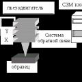 Scanning probe microscope Current state and development of scanning probe microscopy