Microcontrollers MCS-51. Block diagram, ALU, data memory. Microcontrollers of the mcs51 family How to make a port to receive mcs 51
Basic version MCS-51 Brief information. Modern 8-bit microcontrollers (MC) have such real-time control resources, for which expensive multi-chip layouts in the form of separate microcomputer boards were previously used, namely:
● have sufficient memory capacity, its physical and logical division into program memory and data memory (Harvard architecture) and a command system oriented to the execution of control algorithms;
● include all devices (processor, ROM, RAM, input/output ports, interrupt system, bit information processing tools, etc.) required to implement a microprocessor control system with a minimum configuration. In the 1970s, the firm Intel developed and mastered the commercial production of a family of 8-bit MCS-48 microcontrollers, united by a number of common features (digit capacity, command system, a set of basic functional blocks, etc.). The basic version of this family includes:
● 8-bit processor;
● internal program memory (1/2/4K bytes);
● internal data memory (64/128/256 bytes);
● up to 27 internal and 16 external I/O lines;
● one 8-bit timer-counter;
● single-level interrupt system with two request sources. In 1980, the same company developed a new family of eight-bit MCS-51 microcontrollers, which is compatible with the architecture of the MCS-48 family, but has wider capabilities.
The architecture of the MCS-51 family turned out to be so successful that it is still one of the standards for 8-bit MKs to this day. Therefore, MCs of this family, which are widely used in relatively simple control systems, were chosen as the object of study.
Various program preparation tools (compilers, hardware-software emulators, etc.) have been developed for the MCS-51 family, and there are a large number of libraries of standard subroutines. The family includes various modifications of microcircuits (chip versions) of microcontrollers. The articles of this section consider in sufficient detail the basic version of microcontrollers of the MCS-51 family (8051 microcircuit corresponds to the domestic analogue KP1816BE51), the simplest in structural and functional terms and in terms of understanding.
Subsequent series of microcircuits, while maintaining compatibility with the basic version, differ from it in improved manufacturing technology, electrical parameters, additional hardware and functionality. The following articles are devoted to the structural and functional features of subsequent modifications of the MCS-51 family microcircuits.  Generalized block diagram of MCS–51. The composition of the MC, a generalized block diagram of which is shown in fig. 7.1.1, includes:
● 8-bit central processing unit CPU, consisting of ALU, control devices uu and address generator F;
● masked ROM with a capacity of 4K bytes for storing programs;
● 128 bytes RAM for data storage;
● four programmable ports Р0–Р3 for information input-output;
● BPI serial interface block for information exchange with external devices via a two-wire line;
● block of timers/counters BT/C to maintain real-time mode;
● BP interrupt block for organizing interrupts of executable programs. These funds form resident part of the microcontroller located directly on the chip. The MC includes a large number of registers, which are assigned to separate functional blocks and are not shown in the diagram.
The diagram also does not show the control circuits. Bilateral exchange of information between the blocks is carried out via an internal 8-bit data bus SD-8.
By internal 16-bit address bus SHA-16, the address formed in the CPU is displayed in the ROM (12 bits of the address) and in the RAM (8 low bits).
When using external memory, 8 low-order bits of the address are output to port P0 and 3 or 8 high-order bits are output to port P2.
For the logical extension of the interface, the combination of the functions of the port lines is used. As an example, in fig. 7.1.1 dotted line shows the lines of the port P3, performing alternative control signal transmission functions, the purpose of which will be discussed below. To create an internal clock generator, a quartz resonator and two capacitors are connected to the outputs of the microcircuit MK (Fig. 7.1.1). Instead of an internal clock generator, an external oscillator can be used for synchronization. The conventional graphic designation of the microcircuit MK is shown in fig. 7.1.2, designation and purpose of conclusions - in table. 7.1.1. Consider the functional blocks of the MK and the principle of their operation.  Arithmetic-logical device. The arithmetic-logical unit is designed to perform arithmetic (including multiplication and division) and logical operations on eight-bit operands, as well as operations of logical shift, zeroing, setting, etc. The block diagram of the ALU is shown in fig. 7.1.3.
The ALU includes
● parallel eight-bit adder SM combination type with sequential transfer, performing arithmetic (addition and subtraction) and logical (addition, multiplication, disparity and identity) operations;
● battery A, providing the functions of the main arithmetic register;
● register B, used to implement the operations of multiplication and division, or as an additional super-operational register, the functions of which are defined by the user;
● registers(programmatically unavailable) temporary storageРВХ1, РВХ2, intended for receiving and storing operands for the duration of the operation;
● ROM constants ROM storing a correction code for binary-decimal data representation, a mask code for bit operations and a constant code;
● program status word register PSW, fixing the state of the ALU after the operation has been performed. In table. 7.1.2 provides information on the assignment of bits to individual digits of the PSW register. Control device. CPU Control Unit (CU) intended to coordinate the joint work of all MK nodes using the generated clock and control signals. It includes (Fig. 7.1.4): 
● synchronization and control unit USU, which generates clock pulses that set the machine cycles and their individual states (S) and phases (P), and depending on the operating mode of the MK, generates the necessary set of control signals. One, two or four machine cycles are allotted to execute the instruction.
Each machine cycle has six states S1–S6, A each state includes two phase P1, P2, the duration of which is the oscillation period of the clock generator T 0SC .
The duration of the machine cycle is 12T 0SC . All machine cycles are the same, starting with the S1P1 phase and ending with the S6P2 phase.
In addition to clock pulses, the clock device in each machine cycle generates two (sometimes one) strobe signals of the low byte of the ALE address in the form of a positive pulse in phases S1P2-S2P1 and S4P2-S5P1. Timing diagrams in fig. 7.1.5 illustrate the organization of machine cycles; 
● RK command register, command decoder DC and PLA, allowing in each machine cycle to form a set of micro-operations in accordance with the microprogram of the command being executed;
● input-output logic of LVV for receiving and issuing signals that provide information exchange between MC and external devices via ports Р0–Р3;
● The PCON register, which has a single enabled SMOD bit in position PCON.7 to double the data rate of the serial port. The remaining bits are reserved for future use.  Address generator. Address shaper (FA), or PC command counter, intended to form the current 16-bit program memory address and 8/16-bit external data memory address. It includes (Fig. 7.1.6):
● 16-bit buffer B, which communicates between the 8-bit data bus of the SD and the 16-bit internal bus (IS) of the address generator;
● SI increment scheme for increasing the value of the current program memory address by one;
● register for storing the current address of the PTA commands coming from the SI;
● Data pointer register DPTR , consisting of two 8-bit registers DPH and DPL. It serves to store a 16-bit address of the external data memory and can be used as two independent software-accessible RONs;
● RFA address generator register for storing the executive 16-bit program memory address or 8/16-bit external data memory address. This register is also used to transfer data through port P0 to external devices when executing the MOVX @Rm, A and MOVX @DPRT, A instructions.
Data memory. Data memory intended for receiving, storing and issuing information used in the process of program execution. The internal (resident) memory (Fig. 7.1.7) of data consists of RAM with a capacity of 128 bytes, stack pointer SP, address register RAM RA and decoder Dsh.  The SP stack pointer is an 8-bit register that receives and stores the address of the stack location that was last accessed. After reset, the stack pointer is set to address 07H, which corresponds to the beginning of the stack with address 08H. The address register RA together with the decoder Dsh allows access to the required memory cell containing a byte or bit of information.
The MK provides the ability to increase the amount of data memory up to 64 KB by connecting external storage devices. As an example, in fig. 7.1.8 shows the paging of external data memory VPD with a capacity of 2K bytes using instructions like MOVX @
Rm(m = 0; 1). In this case, port P0 operates as a multiplexed address/data bus, three lines of port P2 are used to address an external RAM page, and the remaining five lines can be used as I/O lines.  On fig. 7.1.9 shows the timing diagrams of read and write cycles when the MK is working with external RAM. The diagrams indicate:
● PCN - high byte of the PC command counter;
● DPL, DPH - low and high bytes of the DPTR data pointer register, which is used as an indirect addressing register in the MOVX @DPTR,A and MOVX A,@DPTR instructions;
● P2 SFR - P2 port latches;
● Rm (m = 0, 1) - registers used in MOVX @Rm, A and MOVX A, @Rm instructions as indirect address registers;
● Z - high resistance state;
● D - the period during which data from port P0 is entered into the microcontroller.  Program memory. Program memory is designed to store programs, has its own (separate from data memory) address space and is read-only. It includes a decoder Dsh and ROM (Fig. 7.1.10).
  Program memory is addressed using a 16-bit PC counter, so its maximum capacity is 64K bytes. The internal program memory consists of a ROM with a capacity of 4K bytes and a 12-bit decoder. External memory is connected according to the diagram in fig. 7.1.11.
  If 0 V is applied to the ¯EA pin of the MCU (as shown in Fig. 7.1.11), the internal program memory is disabled. All memory accesses start at address 0000h. When the ¯EA pin is connected to the power supply, the access to the internal program memory at addresses 0000h–FFFFh and to the external program memory at addresses 0FFFh–FFFFh occurs automatically.
To read the external program memory of the MK, the signal ¯PSEN is generated. When working with internal memory, the read signal is not used. When accessing external program memory, a 16-bit address is always formed. The low byte of the address is transmitted through port P0 in the first half of the machine cycle and is fixed by the cut of the ALE strobe in the register. In the second half of the cycle, port P0 is used to enter a data byte from external memory into the MCU.
The high byte of the address is transmitted through the P2 port during the entire time the memory is accessed.
Timing diagrams of read and write cycles during the operation of the MK with external RAM are shown in fig. 7.1.12.  The diagrams indicate:
● PCL OUT - low byte output of the PC command counter;
● PCN OUT - issuance of the high byte of the PC command counter;
● DPH is the high byte of the DPTR data pointer register, which is used as an indirect addressing register in the MOVX @DPTR,A and MOVX A,@DPTR instructions;
● P2 SFR - P2 port latches;
● INS IN - input of instruction (command) byte from program memory;
● ADDR OUT - issuance of the low byte of the external data memory address from the Rm registers (m = 0, 1) or from the DPL register (lower register DPTR). I/O ports. Port assignment. Ports P0, P1, P2, P3 intended to exchange information between the MK and external devices, as well as to perform the following functions:
● low byte of the address А7…A0 is output through port Р0; a byte of data is output from the MK and entered into the MK when working with external program memory and external data memory (with time division);
● high byte of address A15…A8 is output through port P2 when working with external program memory and external data memory (only when using MOVX A,@DPTR and MOVX @DPTR,A commands);
● P3 port lines can be used to perform alternative functions if 1 is entered in the latch of this line, otherwise 0 is fixed at the line output. Alternative functions of P3 port outputs are given in Table. 7.1.3. 
Schematic features of ports
On fig. 7.1.13 shows diagrams for one channel of each of the MK ports, including:
● a latch for fixing the received data bit;
● output amplifying cascade(driver);
● node connection with output stage (except for P2);
● a circuit for transmitting a data bit from the output side of the port, consisting of buffers B2 and B3 (for port P4). The latch is a D-flip-flop, clocked by the internal signal "Write to latch". A bit of data from the direct output of the D-flip-flop can be read by software through buffer B1 by the “Read latch” signal to the line of the internal data bus (SD) of the MK.
Output stage port P0 is an inverter, the features of which are manifested in the fact that the load transistor VT2 opens only when accessing external memory (when transferring addresses and data through the port). In all other modes, the load transistor is closed. Therefore, to use P0 (Fig. 7.1.13, a) as a general-purpose output port, external load resistors must be connected to its outputs. When writing 1 to the port latch, the inverter transistor VT1 is turned off and the external pin of the port P0.X is transferred to a high-resistance state. In this mode, the port pin P0.X can serve as an input. If port P0 is used as a general purpose I/O port, each of its P0.X pins can operate independently as an input or as an output. Output stages ports P1, P2, P3 (Fig. 7.1.13, b, c, d) made according to the circuits of inverters with an internal load resistor, which is used as a transistor VT2.
To reduce the switching time during the transition of the port outputs from state 0 to state 1, an additional transistor VT3 is introduced in parallel with the load transistor VT2. Transistor VT3 with the help of elements in the gate circuit is unlocked for a time equal to two periods of oscillation of the master crystal oscillator (during the phases S1P1, S2P2 of the machine cycle). Output stages ports P0, P2 (Fig. 7.1.13, A, c) using the MX multiplexer can be connected either to the latches or to the internal buses "Address / data" and "Address". The output stage of port P1 (Fig. 7.1.13, 6) is permanently connected to the latch.
If the P3 port pin is an output and its latch contains 1, then its output stage is controlled by the hardware-internal signal “Alternative output function”, which provides the corresponding alternative function, i.e. one of the signals ¯WR, ¯RD or RxD is formed on the external pin. If the port pin is used as an input, then the alternative signal arriving at it (TxD, ¯INT0, ¯INT1, T0, T1) is transmitted to the “Alternative Input Function” internal line.
Port write mode.
When a write to port command is issued, the new value is written to the latch in phase S6P2 and output directly to the port output pin in phase S1P1 of the next machine cycle.
Port Read Mode
Port read commands read information directly from the external pins of the port pins or from latch outputs. In the first case, the data bit from the port output is read programmatically through buffer B2 by the “Read outputs” signal to the line of the internal data bus (SD) of the MK. Note that the signals "Write to latch", "Read latch", "Read pins" are generated by hardware when the corresponding commands are executed.
In the second case, the so-called "Read-Modify-Write" mode is implemented, in which the command reads the latch status signal, modifies it if necessary, and then writes it back to the latch. The Read-Modify-Write mode is implemented when the following commands are executed: ANL, ORL, XRL, JBC; CPL; I.N.C.; DEC; DJNC; MOV PX,Y; CLR PX.Y; SETB PX,Y.
Reading information from latch outputs eliminates errors when interpreting the logic level on a port pin. Read the continuation of the article in.
Currently, various companies produce many modifications and analogues of this family, both by Intel and other manufacturers, the clock frequency and memory size have increased tenfold and continue to increase. The set of built-in LSI modules is also being supplemented; a high-speed resident ADC is built into a large number of modern models, having up to 12, and now there may be more bits. But at the heart of the MSS51 family is the BIS 8051, 80C51, 8751, 87C51, 8031, 80C31 from Intel, the first samples of which were released in 1980.
Microcontrollers of the MCS51 family are made using high-quality n-MOS technology (series 8ХХХ, analogue - series 1816 in Russia and Belarus) and k-MOS technology (series 8ХСХХ, analogue - series 1830). The second character following 8 means: 0 - no EEPROM on the chip, 7 - 4K EEPROM with UV erasure. The third character: 3 - the ROM will be crystallized, 5 - if there is no ROM, then there is a masked ROM on the chip.
And so 80S51 is a k-MOS LSI with a mask ROM on a chip, 8031 is an n-MOS LSI without program memory (ROM, EPROM) on a chip, 8751 is an n-MOS LSI with a resident (located on a chip) RPROM with ultraviolet erasure. We will continue to consider LSI 8751, making, if necessary, reservations about the differences in other circuits, citing the parameters that were published for the first serial LSI. If necessary, you can find additional information about all modern modifications in company directories and technical documentation.
A. General characteristics and pin assignment
The MCS51 family is based on five modifications of MK (having identical main characteristics), the main difference between which is the implementation of program memory and power consumption (see Table 3.1). The microcontroller is eight-bit, i.e. has instructions for processing eight-bit words, has a Harvard architecture, the clock frequency for the basic samples of the family is 12 MHz.
Table 3.1.
|
micro circuits |
Internal program memory, bytes |
Program memory type |
Internal data memory, bytes |
Clock frequency, MHz |
Consumption current, mA |
MK 8051 and 80C51 contain a mask-programmable ROM program memory with a capacity of 4096 bytes and are designed for use in mass production. MK 8751 contains a 4096 byte EPROM with UV erasure and is convenient at the stage of system development when debugging programs, as well as when producing in small batches or when creating systems that require
periodic adjustment.
MK 8031 and 80C31 do not contain built-in program memory. They, like the previously described modifications, can use up to 64 KB of external program memory and are effectively used in systems that require a significantly larger (than 4 KB on a chip) ROM program memory.
Each MK of the family contains a resident data memory with a capacity of 128 bytes with the possibility of expanding the total amount of RAM data up to 64 KB through the use of external RAM ICs.
central eight-bit processor;
4K program memory (8751 and 87C51 only);
128 bytes data memory;
four eight-bit programmable input-output ports;
two 16-bit multimode timers/counters;
a system of autovector interrupts with five vectors and two software-controlled priority levels;
serial interface, including a universal duplex transceiver capable of operating in four modes;
clock generator.
The MK command system contains 111 basic commands with a format of 1, 2, or 3 bytes. The microcontroller has:
32 general-purpose registers RON, organized as four banks of eight registers each with the names R0 ... R7, the choice of a particular bank is determined by the program by setting the corresponding bits in the PSW program status register;
128 software-controlled flags (bit processor, see below);
a set of registers of special functions that control the elements of the MK. The microcontroller has the following operating modes:
one). General reset. 2).Normal operation. 3).Low power mode and idle mode. 4). Programming mode of the resident EPROM, if any.
Here we will focus on the first two modes of operation, a detailed description of the composition and operation of the MC in all modes is given in Appendix P1.
RON and the bit processor zone are located in the address space of the resident RAM with addresses from 0 to 80h.
In the upper zone of addresses of resident RAM are registers of special functions (SFR, Special Function Registers). Their purpose is given in Table. 3.2.
Table 3.2.
|
Designation |
Name | |
|
Battery | ||
|
Register B | ||
|
Program Status Register | ||
|
stack pointer | ||
|
Data pointer. 2 bytes: | ||
|
low byte | ||
|
high byte | ||
|
Interrupt Priority Register | ||
|
Interrupt enable register | ||
|
Timer/Counter Mode Register | ||
|
Timer/Counter Control Register | ||
|
Timer/counter 0. High byte | ||
|
Timer/counter 0. Low byte | ||
|
Timer/counter 1. High byte | ||
|
Timer/counter 1. Low byte | ||
|
Serial port control | ||
|
Serial Buffer | ||
|
Consumption management |
* - registers, allowing bit by bit addressing
Let's take a quick look at the functions of the SFRs listed in Table 3.2.
Battery ACC - accumulator register. Teams designed to work
you with an accumulator, use the mnemonic "A", for example, MOV A, R2 . The mnemonic "ACC" is used, for example, when addressing the accumulator bit by bit. Thus, the symbolic name of the fifth bit of the accumulator when using the A5M51 assembler will be as follows: ACC. 5. .
Register V . Used during multiplication and division operations. For other instructions, register B can be considered as an additional scratchpad register.
Register states programs PSW contains information about the state of the program and is set partly automatically by the result of the operation performed, partly by the user. The designation and purpose of the register bits are given in Tables 3.3 and 3.4, respectively.
Table 3.3.
|
Designation |
Table 3.4.
|
Designation |
Bit Assignment |
Access to the beat |
||||
|
Carry flag. Changes during the execution of a number of arithmetic and logical instructions. |
Hardware or software |
|||||
|
Additional carry flag. Set/cleared by hardware during the execution of add or subtract instructions to indicate a carry or borrow in bit 3 when generating the low nibble of the result (D0-D3). |
Hardware or software |
|||||
|
Flag 0. Flag defined by the user. |
Programmatically |
|||||
|
Programmatically |
||||||
|
Pointer to the bank of working registers |
Programmatically |
|||||
|
Bank 0 addresses (00H - 07H) Bank 1 addresses (08H - 0FH) Bank 2 addresses (10H - 17H) Bank 3 addresses (18H - 1FH) | ||||||
|
overflow flag. Set or cleared by hardware during execution of arithmetic instructions to indicate an overflow condition. |
Hardware or software |
|||||
|
Spare. Contains a read/write trigger that can be used | ||||||
|
Parity bit. Reset or set by hardware every instruction cycle to indicate an even or odd number of battery bits that are in the "1" state. |
Hardware or software |
|||||
Pointer stack SP - An 8-bit register whose content is incremented before data is written to the stack during PUSH and CALL instructions. On initial reset, the stack pointer is set to 07H and the stack area in the data RAM starts at address 08H. If necessary, by redefining the stack pointer, the stack area can be located anywhere in the internal data RAM of the microcontroller.
Pointer data DPTR consists of high byte (DPH) and low byte
(DPL). Contains a 16-bit address when accessing external memory. Can be used
be stored as a 16-bit register or as two independent eight-bit registers.
Port0 - PortZ. Separate bits of the registers of special functions P0, P1, P2, P3 are bits - "latches" of the outputs of ports P0, P1, P2, P3.
Buffer consistent port SBUF represents two separate registers: the transmitter buffer and the receiver buffer. When data is written to SBUF, it enters the transmitter buffer, and writing a byte to SBUF automatically initiates its transmission through the serial port. When data is read from SBUF, it is fetched from the destination buffer.
Registers timer. Register pairs (TH0, TL0) and (TH1, TL1) form 16-
bit counter registers of timer/counter 0 and timer/counter 1, respectively.
Registers management. The special function registers IP, IE, TMOD, TSON, SCON and PCON contain control bits and status bits for the interrupt system, time-
measures/counters and a serial port. They will be discussed in detail below.
RxD TxD INT0 INT1 T0 T1 WR
P1.2 P1.3 P1.4 P1.5 P1.6 P1.7
RST BQ2 BQ 1EA
P3.0 P3.1 P3.2 P3.3 P3.4 P3.5 P3.6 P3.7
P2.0 P2.1 P2.2 P2.3 P2.4 P2.5 P2.6 P2.7
P0.0 P0.1 P0.2 P0.3 P0.4 P0.5 P0.6 P0.7
MC during operation provides:
the minimum execution time for addition commands is 1 µs;
hardware multiplication and division with a minimum execution time of 4 µs.
The MK provides the ability to set the frequency of the internal oscillator using a quartz crystal, an LC chain, or an external oscillator.
The extended command system provides byte and bit addressing, binary and binary-decimal arithmetic, overflow indication and even/odd determination, and the ability to implement a logical processor.
The most important and distinctive feature of the architecture of the MCS51 family is that the ALU can, along with performing operations on 8-bit data types, manipulate single-bit data. Individual software-accessible bits can be set, reset, or replaced by their complement, can be forwarded, checked, and
Fig.3.2. External findings
microcontroller
used in logical calculations. Whereas support for simple data types (when existing
current trend towards increasing word length) may at first glance seem like a step backwards, this quality makes the microcontrollers of the MCS51 family especially suitable for applications that use controllers. The operation algorithms of the latter in their own way assume the presence of input and output boolean variables, which are difficult to implement using standard microprocessors. All these properties are collectively referred to as the Boolean processor of the MCS51 family. This powerful ALU makes the MCS51 family of microcontrollers an equally well-suited instruction set for both real-time control applications and data-intensive algorithms.
The circuit diagram of the microcontroller is shown in fig. 3.2. In the basic version, it is packaged in a 40-pin DIP package. Consider the purpose of the conclusions.
Let's start with the power leads «0 V" and "5 V" , through which it receives the main power. Current consumption is given in table. 3.1.
Conclusion "RST" - reset the microcontroller. When this pin is driven active high, the mode general reset and MK performs the following actions:
Sets the PC instruction counter and all special function registers except port latches P0-P3, stack pointer SP, and register SBUF to zero;
the stack pointer takes the value equal to 07H;
disables all interrupt sources, timer-counters, and serial
selects BANK 0 of RAM, prepares ports P0-RZ for receiving data and determines
shares ALE and PME pins as inputs for external clock;
in the PCON, IP and IE special function registers, reserved bits take on random values, and all other bits are reset to zero;
the SBUF register is set to random values.
sets the latches of ports P0-P3 to "1".
The states of the microcontroller registers after reset are shown in Table 3.5.
Table 3.5.
|
Information |
|
|
indefinite |
|
|
0XXXX0000B for k-MOS 0XXXXXXXB for n-MOS |
The RST output also has an alternative function. Backup power is supplied through it to preserve the contents of the RAM of the microcontroller unchanged when the main one is removed.
conclusions bq1, BQ2 – designed to connect a quartz resonator that determines the clock frequency of the MC.
Conclusion EA` (E xternal A dress – external the address) - designed to activate the mode of reading control codes from external program memory, when an active low level is applied to this output. The output has an alternative purpose (function). It is supplied with the programming voltage of the EPROM in the programming mode.
Conclusion PME (P program M emory E noble – permission memory programs) - designed to control the cycle of reading from the program memory and automatically activated MK in each machine cycle.
Conclusion ALE (A dress L English E noble – permission junior addresses) strobes the output of the low part of the address on port P0. The output is also used when programming the EPROM, while a strobe pulse is applied to it during the programming process.
The MK contains four groups of ports: P0, P1, P2, and P3. These are the remaining 40 pins of the microcontroller. These ports can serve for bit-by-bit input - output of information, but in addition, each of them has its own specialization. The generalized functional diagram of the port is shown in fig. 3.3. The port contains FET output switches connected to the pin, a function switch, a D-latch latch, and control logic. One or zero can be written to the latch on the internal bus of the MK. This information is fed through the function switch to the output keys and the output of the MC. In the state of one, both transistors N and N1 are closed, but N2 is open. In a state of zero, N opens-
Xia, and N2 closes. The moment a port performs the alternate function for which it is specialized, the output latch state is released. The microcontroller can separately read the latch state of the port and the state of its output, set by an external signal. To do this, in the MK assembler there are special commands that activate the corresponding lines. To read the status of a pin to the corresponding port's latch,
be pre-recorded
From internal
Management Latch
Function switch
Vcc 
Weekend
unit. When the “latch reading” line is activated at the output of the “AND” cell to which this line is connected,
her tires MK D Q
Write to latch C Q
latch reading
Port pin
the state of the latch that arrives at the internal bus of the microcontroller, when activated
"reading output" - the state of the external output of the port.
Port P0 – universal bidirectional port
input-output. Behind this port
the function of organizing external busses of addresses and
Rice. 3.3. Functional diagram of the microcontroller port
data to expand the program memory and data memory
microcontroller. When an external program memory is accessed or an external data memory access command is executed, the lower part of the address (A0…A7) is set on the port pins, which is strobed high at the ALE pin. Then, when writing to the data memory, the information being written from the internal bus of the MK is fed to the pins of the P0 port. In read operations, on the contrary, information from the port pins goes to the internal bus. A feature of port P0 is the absence of a “pull-up” transistor N2, which provides power to the output. When a latch is written to the 1 port, it is simply placed in the high impedance state necessary for the data bus to function properly. If it is necessary to power any external devices through the output, external resistors should be provided from the power supply circuits to the port output.
Port P1 – universal bidirectional I/O port without alternative functions.
Port R2 – universal bidirectional I/O port, as an alternative function, issuing the upper part of the address (А8…А15) when accessing external memory.
Port P3 – a universal bidirectional input-output port, each bit of which provides for the performance of various alternative functions. In this case, alternative functions are implemented only if units are written to the port output latches, otherwise the execution of alternative functions is blocked. We list them separately for each bit:
P3.0 – RxD (R head e X ternal D ate, read external data) – input of the built-in serial transceiver.
P3.1 – TxD (T ype e X ternal D ate, transmit external data) – built-in serial transceiver output.
P3.2 – INT0` (INT errupt, interrupt) - external interrupt input 0.
P3.3 – INT1` – external interrupt input 1.
P3.4 – С/T0 – input of zero built-in timer/counter.
P3.5 – C/T1 – input of the first built-in timer/counter.
P3.6 – WR` (W rite, write) - control output of the write cycle in the data memory.
P3.7 – RD` (R ead, read) - output control of the read cycle from the data memory.
Port pins P1, P2 and P3 are capable of outputting about 0.2mA current and receiving 3 mA current at zero, port P0 pins are more powerful and capable of delivering about 0.8mA current at zero and accepting 5 mA current at zero. Brief information about the purpose of the microcontroller pins is given in Table 3.6.
Table 3.6.
|
Designation |
Output Destination | ||
|
8-bit bidirectional P1 port. Address input A0-A7 when checking the internal ROM (RPZU) |
enter exit |
||
|
General reset signal. RAM backup power output from an external source (for 1816) | |||
|
8-bit bidirectional P3 port with additional features |
enter exit |
||
|
Receiver Serial Data - RxD | |||
|
Transmitter Serial Data - TxD | |||
|
External interrupt input 0- INT0` | |||
|
External interrupt input 1-INT1` | |||
|
Timer/counter input 0: - T0 | |||
|
Timer/counter input 1: - T1 | |||
|
Strobe signal output when writing to external data memory: - WR` | |||
|
Strobe signal output when reading from external data memory - RD` | |||
|
Conclusions for connecting a quartz resonator. |
exit entrance |
||
|
General conclusion | |||
|
8-bit bidirectional P2 port. Output address A8-A15 in the mode of operation with external memory. In the internal ROM test mode, the outputs P2.0 - P2.6 are used as the input of the address A8-A14. Conclusion P2.7 - permission to read the ROM. |
enter exit |
||
|
Program memory resolution | |||
|
Address latch enable output. When programming EEPROM signal: PROG |
enter exit |
||
|
Blocking work with internal memory. When programming the EEPROM, the UPR signal is given. |
enter exit |
||
|
8-bit bidirectional port P0. Address/data bus for working with external memory. Data output D7-D0 in the test mode of the internal ROM (RPZU). |
enter exit |
||
|
Power output from a voltage source + 5V |
The basis of the microcontroller (see Fig. 1) is an 8-bit Arithmetic Logic Unit (ALU). The memory of the MK has a Harvard architecture, i.e. logically divided: into program memory - PP (internal or external), addressed by a 16-bit command counter (SC) and data memory - internal (Resident data memory - RPD) 128 (or 256) bytes, as well as external (External data memory – VPD) up to 64 KB. Physically, program memory is implemented on ROM (read only), and data memory is implemented on RAM (data can be written and read).
Reception and delivery of external signals is carried out through 4 eight-bit ports Р0..Р3. When accessing external program memory (EPM) or data memory (VPD), ports P0 and P2 are used as a multiplexed external Address/Data bus. P3 port lines can also perform alternative functions (see Table 1).
The 16-bit DPTR register forms the VPD address or Program Memory base address in the Accumulator conversion instruction. The DPTR register can also be used as two independent 8-bit registers (DPL and DPH) to store operands.
8-bit internal command register (RK) receives the code of the command being executed; this code is decoded by the control circuit, which generates control signals (see Fig. 1).
Access to special function registers - RSF (SFR - in Fig. 1 they are circled with a dotted line) is possible only using direct byte addressing in the address range from 128 (80h) and more.
Resident data memory (RDD) in the first models of microcontrollers of the MCS-51 family had a capacity of 128 bytes. The lower 32 bytes of the RPD are also general-purpose registers - RON (4 banks of 8 RONs each). The program can apply to one of the 8 RONs of the active bank. The selection of the active bank of RONs is carried out by programming two bits in the processor status register - PSW.
Table 1 - MCS-51 pin assignment
| Pin No. | Designation | Purpose |
| 1..8 | P1 | 8-bit quasi-bidirectional I/O port |
| 9 | RST | Reset signal (active level - high); The RST signal resets: the PC and most Special Function Registers (SFRs), disabling all interrupts and timers; selects RON Bank 0; writes "all ones" to ports P0_P3, preparing them for input; writes code 07H to the stack pointer (SP); |
| 10..17 | 8-bit quasi-bidirectional I/O port; after writing to the corresponding bit "1" - performs additional (alternative) functions: Serial port input - RxD; Serial port output - TxD; External interrupt input 0 - ~INT0; External interrupt input 1 - ~INT1; Timer/counter input 0 - T0; Timer/counter input 1 - T1; Strobe output. signal when writing to the VPD - ~ WR; Strobe output. signal when reading from the VPD - ~ RD; |
|
| 18, 19 | X1, X2 | Conclusions for connecting a quartz resonator or LC circuit; |
| 20 | GND | General conclusion; |
| 21..28 | P2 | 8-bit quasi-bidirectional I/O port; or output address A in external memory mode (VPP or VPD); |
| 29 | PME | External Program Memory read strobe, issued only when accessing external ROM; |
| 30 | ALE | External memory address strobe (VPP or VPD); |
| 31 | EA | Disabling the RPP, the level "0" at this input switches the MK to a selection of commands only from the runway ; |
| 39..32 | P0 | 8-bit bidirectional I/O port; when accessing External Memory, it issues addresses A (which are written to an external register by the ALE signal), and then exchanges a byte synchronously with the signal ~PME (for commands) or ~WR,~RD (for data in VPD), when accessing External Memory all units are written to the port register P0, destroying the information stored there; |
| 40 | Ucc | Supply voltage output |
Switching banks of RONs simplifies the execution of subroutines and handling of interrupts, because. it is not necessary to transfer the contents of the RONs of the main program to the stack when calling the subroutine (it is enough to go to another active RON bank in the subroutine).
Access to the RPD is possible using indirect or direct byte addressing (direct byte addressing allows accessing only the first 128 bytes of the RPD).
The extended RPD area (for microcontrollers of the MCS-52 family and subsequent families) from address 128 (80h) to 255 (FFh) can only be addressed using the indirect addressing method.
Table 2 - Block Registers of Special Functions (s f r)
| Mnemo code | Name | |
| 0E0h | *ACC | Battery |
| 0F0h | *B | Register battery expander |
| 0D0h | *PSW | Processor Status Word |
| 0B0h | * P3 | Port 3 |
| 0A0h | * P2 | Port 2 |
| 90h | * P1 | Port 1 |
| 80h | *P0 | Port 0 |
| 0B8h | * IP | Interrupt Priority Register |
| 0A8h | *IE | Interrupt mask register |
| 99h | SBUF | Serial transceiver buffer |
| 98h | * SCON | Serial Port Control/Status Register |
| 89h | TMOD | Timer/Counter Mode Register |
| 88h | * TCON | Timer/Counter Control/Status Register |
| 8Dh | TH1 | Timer 1 (high byte) |
| 8bh | TL1 | Timer 1 (low byte) |
| 8ch | TH0 | Timer 0 (high byte) |
| 8ah | TL0 | Timer 0 (low byte) |
| 83h | DPH | Data Pointer Register (DPTR) (high byte) |
| 82h | DPL | Data Pointer Register (DPTR) (low byte) |
| 81h | SP | Stack pointer register |
| 87h | PCON | Demand power control register |
2. SOFTWARE MODEL MCS–51


COMMAND TYPES MCS–51
Almost half of the commands are executed in 1 machine cycle (MC). With a crystal oscillator frequency of 12 MHz, the execution time for such a command is 1 μs. The remaining commands are executed in 2 machine cycles, i.e. for 2 ms. Only multiplication (MUL) and division (DIV) instructions are executed in 4 machine cycles.
During one machine cycle, there are two accesses to the Program Memory (internal or external) to read two bytes of the instruction, or one access to the External Data Memory (EDM).
3. METHODS (METHODS) OF ADDRESSING MCS–51
1. REGISTER ADDRESSING - 8-bit operand is located in the RON of the selected (active) bank of registers;
2 DIRECT ADDRESSING (indicated by the sign - #) - the operand is located in the second (and for a 16-bit operand and in the third) byte of the command;
3 INDIRECT ADDRESSING (indicated by the - @ sign) - the operand is located in the Data Memory (RPD or VPD), and the address of the memory cell is contained in one of the RONs of indirect addressing (R0 or R1); in the PUSH and POP commands, the address is contained in the stack pointer SP; the DPTR register can contain a VPD address up to 64K;
4 DIRECT BYTE ADDRESSING – (dir) – used to access RPD cells (addresses 00h…7Fh) and special function registers SFR (addresses 80h…0FFh);
5 DIRECT BIT ADDRESSING - (bit) - is used to access separately addressable 128 bits located in RPD cells at addresses 20H ... 2FH and to separately addressable bits of special function registers (see Table 3 and program model);
6 INDIRECT INDEX ADDRESSING (denoted by the @ sign) - simplifies viewing tables in the Program Memory, the PP address is determined by the sum of the base register (PC or DPTR) and the index register (Battery);
7 IMPLICIT (BUILT-IN) ADDRESSING - the instruction code contains an implicit (by default) reference to one of the operands (most often to the Accumulator).
4. PROCESSOR STATUS WORD (PSW) FORMAT

C - Carry (CARY) or borrow flag, also functions as a "boolean accumulator" in bit-operated instructions;
AC – auxiliary (additional) carry flag – set to "1" if the addition command (ADD, ADDC) had a carry from the low order tetrad to the high order (i.e. from the 3rd bit to the 4th bit);
F0 - user flag - set, reset and checked by software;
| RS1 | RS0 | Bank | Address (dir) |
| 0 | 0 | 0 | 00h..07h |
| 0 | 1 | 1 | 08h..0Fh |
| 1 | 0 | 2 | 10h..17h |
| 1 | 1 | 3 | 18h..1Fh |
RS1,RS0 – Register bank selection:
OV - Arithmetic overflow flag; its value is determined by the XOR operation of the input and output carry signals of the most significant bit of the ALU; a single value of this flag indicates that the result of an arithmetic operation in the two's complement code is out of range: –128…+127; when performing the division operation, the OV flag is reset, and in the case of division by zero, it is set; when multiplying, the OV flag is set if the result is greater than 255 (0FFH);
Bit PSW - Reserved, contains a trigger, available for writing or reading;
P - parity flag - is the addition of the number of single bits in the accumulator to an even number; is formed by a combinational circuit (programmatically available only for reading).
The MCS-51 microcontrollers do not have the "Z" flag. But in the conditional jump instructions (JZ, JNZ), the combinational circuit checks the current (zero or non-zero) contents of the Accumulator.
All commands of transfers and exchange of operands can be carried out through the Accumulator (see Fig. 3). Moreover, transfers from / to External Memory (Program Memory or Data Memory) can only be carried out through the Battery.
Most transfers can also be made via a forward byte (dir). There are even dir-to-dir transfers (see Figure 3).
Missing transfers from RON to RON can be implemented as transfers from RON to the forward byte dir (given that the RONs are located in the initial area of the Resident Data Memory, the cells of which can be addressed as dir).
XCH exchange commands allow you to send bytes without destroying both operands.
Arithmetic commands are executed only in the Accumulator. Therefore, the first operand must first be placed in the Accumulator and then add or subtract the second operand. The result is placed in the Accumulator.

The SUBB subtraction command is executed only with a borrow (i.e., the Cary flag is also subtracted from the result). Therefore, in order to execute a subtraction instruction without borrowing, it is necessary to first execute the Clear Flag C (CLRC) instruction.
The instruction for multiplying one-byte operands - MULAB - places a two-byte (16 bit) result: the low byte is in the Accumulator, the high byte is in register B.
The result of executing the instruction for dividing one-byte operands - DIVAB - is placed: the quotient - a Accumulator, the remainder - in register B.
The INC arithmetic instruction adds one to the selected operand. The DEC arithmetic instruction subtracts one from the selected operand. The Accumulator Decimal Correction (DAA) instruction helps you add binary coded decimal (BCD) numbers without converting them to hexadecimal (hex) format. Source operands must be in BCD format, i.e. in each tetrad of one byte there are only numbers from 0 to 9 (there cannot be hexadecimal numbers: A, B, C, D, E, F). Therefore, one byte can contain numbers from 00 to 99 for packed BCD numbers, or numbers from 0 to 9 for unpacked BCD numbers.
The DA A - decimal correction command performs actions on the contents of the Accumulator after adding the BCD numbers in the processor (the numbers were added according to the laws of hexadecimal arithmetic) as follows (see example):

· if the contents of the low-order tetrad of the Accumulator is greater than 9 or the auxiliary carry flag is set (AC = 1), then 6 is added to the contents of the Accumulator (that is, the missing six digits in hex format);
· if after that the content of the high order of the Accumulator is greater than 9 or the flag C is set, then the number 6 is added to the high order of the Accumulator.
The decimal correction instruction DA A is not used after the increment instruction (INC) because the increment instruction does not affect (change) the C and AC flags.
Logic commands:
Logical "AND" - ANL,
Logical "OR" - ORL,
The XOR logical command - XRL - is executed in the Accumulator (as well as arithmetic), but it is possible to execute logical commands also in the direct address byte (dir). In this case, the second operand can be:
in the battery or
An immediate operand in an instruction.
Rotation instructions (RR A, RL A) and rotation instructions through the CARY flag (RRC A, RLC A) rotate the contents of the Accumulator by 1 bit. Bit operands are sent only through the C flag.
UDC 681.5, 681.325.5 (075.8)
BBK 32.973.202-018.2 i 73
Shcherbina A. N.Computing machines, systems and networks. Microcontrollers and microprocessors in control systems: Cheb. allowance / A.N. Shcherbina, P.A. Nechaev-SPb.: From the Polytechnic. un-ta, 2012.-226 p.
Corresponds to the content of the state educational standard for areas of training and specialties in the field of management in technical systems, electric power and electrical engineering and the content of the exemplary curriculum of the discipline "Computers, systems and networks".
The fundamental questions of the logical organization of microprocessor systems are considered on the example of the basic architecture of the MCS-51 microcontroller family from Intel. The technology of programming microcontrollers in Assembler and SI languages is described.
It can be useful for students and teachers of higher technical institutions, specialists in automation of technological processes and production equipment, as well as for design engineers of microprocessor systems.
It also corresponds to the content of the state educational standard of the disciplines "Microcontrollers and microprocessors in control systems" and "Electronic devices of automation" for bachelor's, engineering and master's training in the direction 140400 "Electric power and electrical engineering".
Published by decision of the editorial and publishing council
St. Petersburg State Polytechnic University.
© Shcherbina A. N., Nechaev P. A., 2012
© St. Petersburg State
polytechnic university, 2012
ISBN 978-5-7422-3553-8
Introduction.. 7
Chapter 1. Architecture of the MCS51 family. 10
1.1 General characteristics 10
1.2 Block diagram 11
1.3 8051 microcontroller pin assignment 15
1.4 Memory organization 17
1.4.1 Program memory (ROM) 18
1.4.2 Data memory (RAM) 19
1.4.3 Registers of special functions. twenty
1.4.4 Flag Register (PSW) 23
1.5 Control and synchronization device 26
1.6 Organizing I/O ports 27
1.6.1 General information. 27
1.6.2 Alternative functions. 27
1.7. Timers / counters of microcontrollers of the 8051 family. 28
1.7.1. Structure of timers-counters. 28
1.7.2 Operating modes of timers-counters. thirty
1.8. Serial port 32
1.8.1. The structure of the serial port. 32
1.8.2. Transceiver control/status register SCON.. 34
1.8.3. Power control register PCON.. 36
1.9. Interrupt System 37
1.9.1. The structure of the interrupt system. 37
1.9.2 Execution of the interrupt routine. 40
Chapter 2 Features of 80C51GB.. microcontroller 42
2.1 Features 42
2.2 I/O ports P0-P5 43
2.2.1 Operation of I/O ports. 43
2.2.2 Writing to port.. 46
2.3 Features of the 8XC51GB.. interrupt system 49
Enable/disable interrupts. 50
Interrupt priority management. 51
external interrupts. 54
2.3. ADC node 56
2.4. Hardware watchdog 61
2.5. Clock Failure Detection 63
2.6. Matrix of programmable counters RSA 64
2.6.1. Structure PCA.. 64
2.6.2. PCA Counter Mode Register (CMOD) 66
2.6.3. PCA counter control register (CON) 67
2.6.4. Compare/fix modules. 68
2.7. Enhanced Serial Port 76
2.8. Timers/Counters 79
Pin assignment of 8XC51GB.. group microcontrollers 86
Chapter 3 Programming MK 8051GB.. 89
3.1. Software model 89
3.2 Data types 93
3.3 Ways of addressing data 93
3.4 Command system 95
3.4.1 General characteristics. 95
3.4.2 Command types. 96
3.4.3 Types of operands. 97
3.4.4 Microcontroller data transfer commands. 98
3.4.5 Arithmetic instructions 8051.101
3.4.6 8051 MCU Logic Commands. 104
3.4.7 8051 Bit Operation Commands. 106
3.5 Debugging programs 111
Chapter 4. ASM-51 Programming Language. 112
4.2 Writing program text 113
4.3 Language alphabet. 114
4.4 Identifiers. 115
4.5 Numbers 117
4.6 Directives 118
4.7 Implementation of subroutines in ASM51 122
4.7.1 The structure of the subroutine-procedure in the ASM51 language. 122
4.7.2 Passing parameter variables to a subroutine. 123
4.7.3 Implementation of subprograms-functions in the ASM51 language. 123
4.7.4 Implementation of interrupt handling routines in the ASM51 language. 124
4.8 Structured programming in assembly language. 125
4.9 Peculiarities of translation of multi-module programs.. 126
4.10 Using segments 128
4.10.1 Partitioning the MK memory into segments .. 128
4.10.2 Absolute memory segments. 129
4.10.2 Relocatable memory segments. 131
Chapter 5. The C-51 Programming Language. 134
5.1 General characteristics of the language 134
5.3 Structure of C-51 programs 136
5.3. Elements of the C-51 programming language 138
5.3.1. Symbols.. 138
5.3.2. Lexical units, separators and the use of spaces. 141
5.3.3 Identifiers.. 142
5.3.4 Keywords. 143
5.3.5 Constants.. 143
5.4. Expressions in language statements 146
programming C-51 146
5.5. Operation Priorities 148
5.6. C-51 programming language statements 149
5.6.1. declaration operators. 150
5.6.2 Executable statements.. 150
5.6.3 Assignment operator. 151
5.6.4 Conditional statement. 151
5.6.5 Structural operator (). 152
5.6.6 The for loop statement. 152
5.6.7 Loop statement with condition check up to the while loop body. 153
5.6.8 Loop statement with condition check after loop body do while. 154
5.6.9 The break statement. 155
5.6.10 The continue statement. 155
5.6.11 Switch selection statement. 155
5.6.12 The goto operator. 157
5.6.13 Operator expression. 158
5.6.14 Return statement from subroutine return. 158
5.6.15 Empty statement. 158
5.7. Declaring Variables in the C-51 Programming Language. 159
5.7.1. Variable declaration. 159
5.7.3 Integer data types. 161
5.7.4 Floating point numbers. 162
5.7.5 Variables of enumerated type. 162
5.7.6. Declaring arrays in the C-51 programming language. 164
5.7.7. Structures.. 165
5.7.8. Associations (mixtures) 166
5.8. Using Pointers in C-51 167
5.8.1. Declaring pointers. 167
5.8.2. Untyped pointers. 168
5.8.3. Memory dependent pointers. 169
5.9. Declaring new types of variables 169
5.10. Data initialization 170
5.11. Using subroutines in the C-51 programming language. 170
5.11.1. Definition of subroutines.. 171
5.11.2. Subprogram parameters .. 173
5.11.3. Advance declaration of subroutines.. 174
5.11.4 Calling subroutines.. 176
5.11.5 Recursive subprogram call.. 176
5.11.6 Interrupt routines. 177
5.11.7 Scope of Variables and Subroutines.. 178
5.12. Multi-module programs 179
Chapter 6. Preparing Programs in the Keil μVision2 Integrated Development Environment. 182
6.1 Creating an ASM-51 project 182
6.2 Example of creating a C project for a training controller in the Keil μVision2 IDE 188
Chapter 7 Learning Controller Description .. 199
7.1. Controller structure 199
7.2. Address space 200
7.2.1. Memory allocation. 200
7.2.2 External memory. 201
7.2.3. Internal data memory. 202
7.3. I/O port allocation 202
7.4. Serial port………………………………...203
7.5. Working with LCD 205
7.6. Controller panels…………………………………………………213
APPENDIX P2 STRUCTURE OF THE REPORT ON LABORATORY WORK……..217
Appendix P3 Codes of machine commands. 217
References... 224
Introduction
In the development of specialties related to the automation of technological processes and production, the study of microcontrollers is one of the important sections.
There is a continuous development and emergence of more and more 16- and 32-bit microcontrollers and microprocessors in the world, but the largest share of the world microprocessor market still remains with 8-bit devices. According to all forecasts of analytical companies for the near future, the leading position of 8-bit microcontrollers in the world market will continue.
Currently, among all 8-bit microcontrollers, the MCS-51 family is the undisputed leader in the number of varieties and the number of companies producing its modifications. It takes its name from the first representative of this family - the microcontroller 8051. A successful set of peripherals, the possibility of a flexible choice of external or internal program memory and an affordable price ensured this microcontroller was a success in the market.
Advantages of the MCS-51 family:
architecture, which is the de facto standard;
The extreme breadth of the family and the variety of opportunities;
Availability of high-performance and extended versions of processors;
a significant number of freely available software and hardware developments;
ease of hardware programming, including in-circuit programming;
low cost and availability of basic chips;
Availability of specialized versions of controllers for special conditions of use
Availability of versions of controllers with a reduced level of electromagnetic interference;
· wide popularity among the developers of the older generation, both in the world and in the CIS countries;
Support of architecture by leading educational institutions of the world.
And, finally, the main advantage: having mastered the basic chip of the family, it is easy to start working with such computing "monsters" as Cygnal, Dallas Semiconductor, Analog Devices, Texas Instruments microcontrollers.
The MCS-51 family includes a whole range of microcircuits from the simplest microcontrollers to quite complex ones. To date, there are more than 200 modifications of microcontrollers of the 8051 family, produced by almost 20 companies. Every year there are more and more variants of representatives of this family.
The main areas of development are:
increase in speed (increasing the clock frequency and redesigning the architecture);
reduction of supply voltage and power consumption;
· increase in the amount of RAM and FLASH memory on a chip with the possibility of in-circuit programming;
· introduction of complex devices such as drive control systems, CAN and USB interfaces, etc. into the microcontroller periphery.
Microcontrollers of the MCS-51 family allow you to perform both the tasks of controlling various devices and implementing individual nodes of the analog circuit. All microcircuits of this family work with the same command system. Most of them are carried out in the same cases with the same pinout (numbering of the legs for the case). This makes it possible to use microcircuits of different manufacturers for the developed device without altering the circuit diagram of the device and the program.
The main manufacturers of varieties of the 51st family in the world are Philips, Siemens, Intel, Atmel, Dallas, Temic, Oki, AMD, MHS, Gold Star, Winbond, Silicon Systems and a number of others.
Characteristics of analogues of microcontrollers of the MCS-51 family (Intel 8XC51FA, 8XC51GB, 80C152) with advanced features are given in Table. IN 1.
Table B.1
| RAM | ROM | SAR | ADC | WDT | T/C | Afterbirth. Channels | Peculiarities | |
| Atmel: AT89C2051 | ||||||||
| - | - | - | - | UART | Flash 2 Kb | |||
| AT89C4051 | - | - | - | - | UART | Flash 4 Kb | ||
| AT89S4D12 | 128K | - | - | - | UART, SPI | Flash 4 Kb | ||
| DALLAS Semiconductor: DS5000FP | ||||||||
| - | - | - | + | UART | bootstrap loader | |||
| DS5001FP | - | - | - | + | UART | bootstrap loader | ||
| DS8xC520 | 16K | - | - | + | 2xUART | 2DPTR | ||
| SIEMENS: C505C | ||||||||
| 16K | - | + | + | UART, CAN | 8DPTR | |||
| C515C | 64K | - | + | + | UART+SSC+CAN | 4 PWM, 8 DPTR | ||
| Philips: *89C51RA+ | ||||||||
| - | + | - | + | UART | 2 DPTR, lvl 4 interrupt, clock out, Flash 8K | |||
| P51XAG1x | 8K | - | - | + | 2 UARTs | |||
| Intel: 8xC51RA | ||||||||
| 8K | - | + | + | UART | 4 levels IRQ, clock out | |||
| 8XC196KC | 64K | 16K | - | + | - | UART | 3 PWM | |
| 80C196KB | 64K | 8K | - | + | - | UART | PWM |
Chapter 1 MCS51 Family Architecture
8-bit single-chip microcontrollers of the MCS-51 family have gained great popularity among developers of microprocessor control systems due to their well-designed architecture. The microcontroller architecture is a set of internal and external software-accessible hardware resources and a system of commands. The architecture of the MCS-51 family is largely determined by its purpose - the construction of compact and low-cost digital devices. Microcontrollers that perform all the functions of a microcomputer using a single microcircuit are called single-chip computers (OEVMs).
Intel has released about 50 models based on the operating core of the Intel 8051 microcontroller. At the same time, many other companies, such as Atmel, Philips, began production of their microcontrollers developed in the MCS-51 standard.
General characteristics
The main characteristics of the family:
· 8-bit central processing unit (CPU), focused on the control of executive devices;
· The CPU has a built-in circuit of 8-bit hardware multiplication and division of numbers;
The presence in the instruction set of a large number of operations for working with directly addressable bits makes it possible to talk about a processor for working with bit data (Boolean processor);
internal (on-chip) program memory of a mask or reprogrammable type, which has a volume of 4 to 32 Kb for various crystals, it is absent in some versions;
· at least 128 bytes of data resident RAM, which is used for organization, register banks, stack, and user data storage;
· at least 32 bidirectional interface lines (ports), individually configured for input or output of information;
· two 16-bit multi-mode counters/timers used to count external events, organize time delays and clock the communication port;
· Bidirectional duplex asynchronous transceiver (UART) designed to organize communication channels between the microcontroller and external devices with a wide range of information transfer rates. There are means for hardware-software integration of microcontrollers into a connected system;
· a two-level priority interrupt system that supports at least 5 interrupt vectors from 4 internal and 2 external event sources;
built-in clock generator.
Structural scheme
The block diagram of the controller is shown in Figure 1.1 and consists of the following main functional units: a control unit, an arithmetic logic unit, a timer/counter unit, a serial interface and interrupt unit, a program counter, data memory, and program memory. Bilateral exchange is carried out using an internal 8-bit data highway. Almost all representatives of the MCS-51 family are built according to this scheme. Various microcircuits of this family differ only in special-purpose registers (including the number of ports).
Control and synchronization unit (Timing and Control)- designed to generate synchronizing and control signals that ensure the coordination of the joint operation of the OEVM units in all permissible modes of its operation. The control unit includes:
device for forming time intervals;
input-output logic;
instruction register;
electricity consumption management register;
command decoder, computer control logic.

Rice. 1.1. Structural diagram of the I8051 controller.
Time slotting device is intended for generation and output of internal synchronization signals of phases, cycles and cycles. The number of machine cycles determines the duration of instruction execution. Almost all OEVM commands are executed in one or two machine cycles, except for the multiplication and division instructions, the duration of which is four machine cycles. Let us denote the frequency of the master oscillator through F g. The duration of the machine cycle is 12/F g, or 12 periods of the signal of the master oscillator. The input-output logic is designed to receive and issue signals that ensure the exchange of information with external devices through the input/output ports P0-P3.
Command register is designed to record and store an 8-bit operation code of the command being executed. The operation code, with the help of a command decoder and computer control logic, is converted into a microprogram for command execution.
Demand Control Register (PCON) allows you to stop the operation of the microcontroller to reduce power consumption and reduce the level of interference from the microcontroller. An even greater reduction in power consumption and noise reduction can be achieved by stopping the master oscillator of the microcontroller. This can be achieved by toggling bits in the PCON demand control register. For the nMOS manufacturing option (1816 series or foreign chips that do not have the letter "c" in the middle of the name), the power control register PCON contains only one bit that controls the baud rate of the SMOD serial port, and there are no power consumption control bits.
Arithmetic Logic Unit (ALU) is a parallel eight-bit device that provides arithmetic and logical operations. ALU consists of:
accumulator registers, holding registers TMP1 and TMP2;
ROM constants;
adder;
additional register (register B);
battery (ACC);
program status register (PSW).
Register accumulator and holding registers- eight-bit registers designed to receive and store operands for the duration of operations on them. These registers are not programmatically accessible.
ROM constants ensures the development of a correcting code for binary-decimal data representation, a mask code for bit operations, and a constant code.
Parallel 8-bit adder is a combination-type circuit with sequential transfer, designed to perform arithmetic operations of addition, subtraction and logical operations of addition, multiplication, inequivalence and identity.
Register B- an eight-bit register used during multiplication and division operations. For other instructions, it can be considered as an additional scratchpad register.
Battery- an eight-bit register designed to receive and store the result obtained when performing arithmetic-logical operations or shift operations
Serial Interface and Interrupt Block (SIP) designed to organize the input - output of sequential information flows and the organization of the program interrupt system. The block includes:
buffer PIP;
control logic;
control register;
transmitter buffer;
receiver buffer;
serial port transceiver;
interrupt priority register;
interrupt enable register;
interrupt flag processing logic and vector generation scheme.
Program Counter is designed to form the current 16-bit address of the internal program memory and the 8/16-bit address of the external program memory. The program counter consists of a 16-bit PC buffer, a PC register, and an increment circuit (incrementing content by 1).
Data memory (RAM) is intended for temporary storage of information used during the execution of the program.
Ports P0, P1, P2, P3 are quasi-bidirectional input-output ports and are designed to ensure the exchange of information between the OEVM and external devices, forming 32 input-output lines.
Program Status Register (PSW) is designed to store information about the state of the ALU during the execution of the program.
Program memory (EPROM) designed to store programs and is a read-only memory (ROM). Various microcircuits use masked, UV-erasable or FLASH ROMs.
Data Pointer Register (DPTR) designed to store a 16 - bit address of external data memory.
Stack pointer (SP) is an eight-bit register designed to organize a special data memory area (stack), in which you can temporarily store any memory cell.
1.3 8051 microcontroller pin assignment(Fig. 1.2)
· U ss - the potential of the common wire ("earth");
U cc - main supply voltage +5 V;
· X1,X2 - conclusions for connection of a quartz resonator;
· RST - input of the general reset of the microcontroller;
PSEN - external program memory permission, issued only when accessing external ROM;
· ALE - external memory address strobe;
· EA - disable internal program memory; level 0 at this input causes the microcontroller to execute the program only from the external ROM; ignoring the inner (if the latter exists);

Rice. 1.2. Pin assignment 8051.
P1 - eight-bit quasi-bidirectional input/output port, each bit of the port can be programmed both for input and output of information, regardless of the status of other bits;
· P2 - an eight-bit quasi-bidirectional port, similar to P1, the pins of this port are used to issue address information when accessing external program or data memory (if 16-bit addressing of the latter is used). In addition, port pins are used when programming to enter the high-order bits of the address into the microcontroller;
· РЗ - an eight-bit quasi-bidirectional port, similar to Р1, the pins of this port can perform a number of alternative functions that are used in the operation of timers, a serial I / O port, an interrupt controller, and external program and data memory;
· P0 - multiplexed eight-bit bidirectional port of input-output of information, through this port at different points in time the low byte of the address and data are output.
Memory organization
The entire MCS-51 series has a Harvard architecture, i.e. separate program and data memory address spaces. The memory structure is shown in fig. 1.3.
The amount of internal (resident) program memory (ROM, EPROM or OTP ROM) located on a chip, depending on the type of microcircuit, can be 0 (ROMless), 4K (base chip), 8K, 16K or 32K. If necessary, the user can expand the program memory by installing an external ROM. Access to internal or external ROM is determined by the value of the signal at the EA (External Access) pin:
EA=V cc (supply voltage) - access to internal ROM;
EA=V ss (ground potential) - access to external ROM.
For ROMless chips, the EA pin must be permanently connected to V ss .
 |  |
Rice. 1.3. Memory organization of the MCS-51 family
External ROM read strobe - (Program Store Enable) is generated when accessing external program memory and is inactive during access to the ROM located on the chip. The low program memory address area is used by the interrupt system. The 8051 base chip architecture supports five interrupt sources:
two external interrupts;
two interrupts from timers;
interrupts from the serial port.
On fig. 1.4 shows a map of the lower area of program memory.

Rice. 1.4. Map of the lower area of program memory
Program memory (ROM)
For microcontrollers of the 8051 family, program memory and data memory are independent and independent devices, addressed by various commands and control signals.
The amount of built-in program memory located on the 8051 microcontroller chip is 4 KB (in the family up to 32). When accessing external program memory, all 8051 microcontrollers always use a 16-bit address, which provides them with access to 64 KB of ROM. The microcontroller accesses program memory when reading the opcode and operands (using the PC program counter), as well as when executing commands to copy a byte from program memory to the accumulator. When executing data copy commands, the addressing of the program memory cell from which data will be read can be carried out using both the PC counter and a special two-byte data pointer register DPTR.
Data memory (RAM)
The amount of on-chip data memory is 128 bytes. The external data memory can be up to 64 KB. The first 32 bytes are organized into four banks of general purpose registers, designated respectively bank 0 - bank 3. Each of them consists of eight registers R0-R7. At any time, the program is available, with register addressing, only one bank of registers, the number of which is contained in the third and fourth bits of the PSW program status word.
8051 Microcontroller Bit Area Addresses
Table 1.1
| Byte address (Hex) | Bit addresses by bit | |||||||
| D7 | D6 | D5 | D4 | D3 | D2 | D1 | D0 | |
| 2F | 7F | 7E | 7D | 7C | 7B | 7A | ||
| 2E | ||||||||
| 2D | 6F | 6E | 6D | 6C | 6B | 6A | ||
| 2C | ||||||||
| 2B | 5F | 5E | 5D | 5C | 5B | 5A | ||
| 2A | ||||||||
| 4F | 4E | 4D | 4C | 4B | 4A | |||
| 3F | 3E | 3D | 3C | 3B | 3A | |||
| 2F | 2E | 2D | 2C | 2B | 2A | |||
| 1F | 1E | 1D | 1C | 1B | 1A | |||
| 0F | 0E | 0D | 0C | 0B | 0A | |||
| 20h |
The remaining address space can be configured by the developer at his own discretion: it can accommodate the stack, system and user data areas. Data memory cells can be accessed in two ways. The first way is direct addressing of a memory cell. In this case, the cell address is the operand of the corresponding instruction. The second method is indirect addressing using pointer registers R0 or R1: before executing the corresponding command, one of them must contain the address of the cell to which it is necessary to access.
To access external data memory, only indirect addressing is used using registers R0 and R1 or using the 16-bit pointer register DPTR.
Part of the data memory is a bit area, it has the ability to use special bit commands to address each digit of the memory cells. The address of directly addressable bits can also be written in the form (ByteAddress).(Bit). The correspondence between these two addressing methods can be determined from Table. 1.1.
The OMEVM command system provides great data processing capabilities, provides the implementation of logical, arithmetic operations, as well as real-time control. Implemented bitwise, tetrad (4 bits), byte (8 bits) and 16-bit data processing.
LSI family MCS-51 - 8-bit OMEVM: ROM, RAM, special-purpose registers, ALU and external buses have a byte organization. The two-byte data is used only by the pointer register (DPTR) and the program counter (PC). It should be noted that the data pointer register can be used as a two-byte register DPTR or as two single-byte special-purpose registers DPH and DPL. The program counter is always used as a two-byte register.
The OMEVM command set has 42 command mnemonics for specifying 33 functions of this system.
The syntax of most assembly language instructions consists of a function mnemonic followed by operands specifying addressing methods and data types. Different data types or addressing modes are determined by the set operands, not by changes in mnemonic notation.
The command system can be conditionally divided into five groups:
There are the following types of source operand addressing:
- Indirect register addressing by sum of base and index registers
Table of designations and symbols used in the command system
| Designation, symbol | Purpose |
| A | Battery |
| Rn | Registers of the currently selected register bank |
| r | The number of the loaded register specified in the command |
| direct | Directly addressable 8-bit internal data location address, which can be an internal data RAM location (0-127) or SFR (128-255) |
| @rr | Indirectly addressable 8-bit internal data RAM location |
| data8 | 8-bit immediate data included in CPC |
| dataH | MSBs (15-8) of immediate 16-bit data |
| dataL | Low bits (7-0) of immediate 16-bit data |
| addr11 | 11-bit destination address |
| addrL | Least significant bits of the destination address |
| disp8 | 8-bit signed offset byte |
| bit | Directly addressable bit whose address contains the CPC located in the internal data RAM or SFR |
| a15, a14...a0 | Destination address bits |
| (X) | The content of the X element |
| ((X)) | Content at the address stored in element X |
| (X)[M] | Discharge M element X |
+ - * AND OR XOR /X |
Operations: additions subtraction multiplication division logical multiplication (AND operation) logical addition (OR operation) addition modulo 2 (XOR) element X inversion |
Function mnemonics are uniquely associated with specific combinations of addressing methods and data types. In total, 111 such combinations are possible in the command system. The table shows a list of commands sorted alphabetically.
| Mnemonics | Function | Flags |
| ACALL team | Absolute subroutine call | |
| Addition | AC, C, OV | |
| Addition with carry | AC, C, OV | |
| AJMP team | Absolute transition | |
| Logic "AND" | ||
| Logical "AND" for variable-bits | C | |
| Compare and jump if not equal | C | |
| Team CLR A | Battery reset | |
| CLR team |
Reset bit | C, bit |
| CPL Team A | Battery inversion | |
| CPL team |
Bit inversion | C, bit |
| Team DA A | Accumulator decimal correction for addition | AC, C |
| DEC Team<байт> | Decrement | |
| Team DIV AB | Division | C, OV |
| Team DJNZ<байт>, <смещение> | Decrement and jump if non-zero | |
| Team I.N.C.<байт> | Increment | |
| Team INC DPTR | Data pointer increment | |
| Team J.B. |
Jump if bit is set | |
| Team JBC |
Branch if the bit is set and reset this bit | |
| Team J.C. |
Jump if carry is set | |
| JMP @A+DPTR command | Indirect transition | |
| JNB team |
Jump if bit is not set | |
| Team JNC |
Jump if no transfer is set | |
| Team JNZ |
Jump if accumulator content is non-zero | |
| Team JZ |
Jump if accumulator content is 0 | |
| LCALL Team | long call | |
| Team LJMP | long transition | |
| Forward variable-byte | ||
| Send data bit | C | |
| Command MOV DPTR,#data16 | Load data pointer with 16-bit constant | |
| MOVC instruction A,@A+( |
Move byte from program memory | |
| Send to external memory (from external memory) data | ||
 Selecting a GIS processing program
 Calculation and analysis of an electric circuit of an alternating current
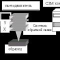 Scanning probe microscope Current state and development of scanning probe microscopy